Students can Download 1st PUC Electronics Model Question Paper 1 with Answers, Karnataka 1st PUC Electronics Model Question Papers with Answers helps you to revise the complete syllabus.
Karnataka 1st PUC Electronics Model Question Paper 1 with Answers
Time: 3.15 Hours
Max Marks: 70
Note :
- Question paper contains four parts.
- Part-A is compulsory, Part-D contains two subparts (a) problems (b) essay type questions.
- Explanation without circuit diagram, wherever necessary, does not carry mark.
PART-A
Answer all questions. Each question carries one mark. (10 × 1 = 10)
Question 1.
Who discovered the electron?
Answer:
J.J. Thomson.
Question 2.
Mention commercial unit of electrical energy.
Answer:
Kilowatt-hour (KWH).
Question 3.
What is a node?
Answer:
Node is a point in a circuit where more than two resistors meet.
Question 4.
Mention one donor impurity atom.
Answer:
Arsenic.
![]()
Question 5.
Define S.I. unit of electrical current.
Answer:
The current in a conductor is said to be one ampere if one coulomb of charge flows through a cross-section of a conductor in one second.
Question 6.
Name the regions of a transistor in the increasing order of their doping level.
Answer:
Base, collector, emitter.
Question 7.
Name the different regions of output characteristics of a transistor.
Answer:
- Saturation region,
- Cutofifregion,
- Active region.
Question 8.
In operating a transistor inactive region, how is the collector-base junction biased?
Answer:
Reverse biased.
![]()
Question 9.
Which property of a diode is used for rectification.
Answer:
Unidirectional property.
Question 10.
What is a NAND gate?
Answer:
NAND gate is a logic circuit whose output is low only when all its inputs are HJGH.
PART-B
Answer any five questions. Each question carries two marks. (5 × 2 = 10)
Question 11.
Write any two applications of an oscilloscope.
Answer:
- to measure AC/DC voltages
- to measure frequency.
Question 12.
Mention the expressions for
(i) frequency in terms of time period and
Answer:
Frequency = \(\frac{1}{\text { time period }}\)
(ii) peak voltage in terms of rms voltage.
Answer:
Vp = \(\sqrt{2}\) × Vrms
Question 13.
Draw the circuit diagram of the RC low pass filter. Write the expression for its cutoff frequency.
Answer:
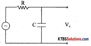
Cutoff frequency fc = \(\frac{1}{2 \pi R C}\)
Question 14.
Define depletion region and potential barrier.
Answer:
The depletion region is the region near the p-n junction where mobile charge carriers electrons and holes are emptied.
A potential barrier is a small voltage developed at the p-n junction which obstructs the diffusion of the mobile charge carriers namely electrons and holes.
![]()
Question 15.
Obtain the relation between α and β of a transistor.
Answer:
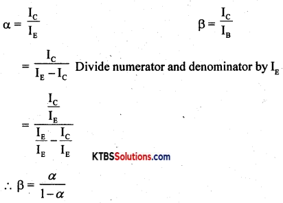
Question 16.
What is a phototransistor? Draw its symbol
Answer:
The phototransistor is a transistor that is sensitive to incident light on it.
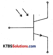
Symbol of phototransistor
Question 17.
Write how l’s and 2’s complements of a number are obtained.
Answer:
1 ‘s complement of a number is obtained by changing 0 to 1 and 1 to 0.
2’s complement of a number is obtained by adding 1 to 1 ’s complement of the binary number.
Question 18.
Prove that A + A̅B = A + B
Answer:
LHS = A + A̅B
= A.1 + A̅B
= A(1 + B) + A̅B
= A + B.1
= A + B
= RHS
PART-C
Answer any five questions. Each question carries three marks. (5 × 3 = 15)
Question 19.
Write a note on the role of electronics in medical science.
Answer:
Electronic devices are widely used iñ medical science in the diagnosis and treatment of different ailments. The electronic deviçes commonly used in the field of medical science are Electrocardiographs (ECG), X-rays, ultrasound scanning machines, endoscopy, glucometer.
Question 20.
State and explain Kirchoff’s Voltage Law.
Answer:
- The sum of the currents flowing towards a node in a circuit is equal to the sum of the currents away from the node.
- The algebraic sum of EMFs in any closed loop of a network is equal to the algebraic sum of IR drops in that loop.
![]()
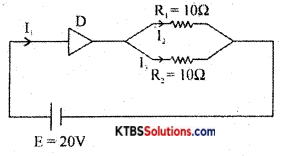
Question 21.
Find the currents in the following circuit assuming the diode to be an ideal diode.
Answer:
Question 22.
Explain the construction of electrolytic capacitor.
Answer:
The electrolytic capacitor has two sheets of aluminium foils separated by a layer of absorbent paper or plastic gauge. The gauge is soaked in a paste of electrolyte of borax or phosphate.
They are rolled up and placed in a cylindrical aluminium container. The inner foil acts as the positive plate and the negative terminal is attached to an aluminium container that contacts the outer foil. After assembling, a DC voltage is applied to the capacitor terminals oxide on the surface of the positive plate next to the electrolyte.
The oxide layer acts as the dielectric. As the oxide layer formed is extremely thin which acts as a dielectric material, these capacitors have a large capacitance value. An electrolytic capacitor is polarity sensitive. If connected wrongly, gas forms within the electrolyte and the capacitor may be damaged due to gas formed may lead to an explosion. Hence electrolytic capacitors are polarity sensitive.
Their capacitance value ranges from 1 μF to 0.01 μF with a vo1tag rating of 50V to 10KV. Electrolytic capacitors are suitable for high-frequency applications and ¡n radio frequency and microwave systems.
![]()
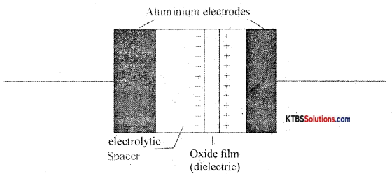
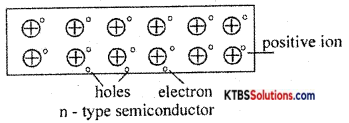
Question 23.
Explain how n-type material is obtained.
Answer:
n-type semiconductors are the semiconductors that are doped with pentavalent impurities like phosphorous, antimony and arsenic. Each pentavalent atom donates one electron and hence is called donor impurity.
When a pentavalent atom is added, the four valence electrons form covalent bonds with neighbouring four silicon atom and its fifth electron becomes a free electron. The free-electron produced by the pentavalent atom does not create a hole.
When few covalent bonds break due to thermal energy, electrons and holes are created. Thus there will be a large number of free electrons. Hence in n-type material, there are electrons as majority charge carriers and holes as minority charge carriers. The pentavalent impurity atom becomes an immobile positive ion after donating an electron.
The n-type material is electrically neutral because the number of free electron equals the sum of positive holes and positive ions.
Question 24.
What is a bleeder resistor? Mention its advantages.
Answer:
A bleeder resistor is a resistor connected across filter output so as to maintain minimum current through the choke at all times.
It is also used to
- improve voltage regulation of the power supply.
- provide a path for the filter capacitor to discharge so as to avoid the possibility of electric shock to technicians.
Question 25.
Write any three differences between germanium and silicon diodes.
Answer:
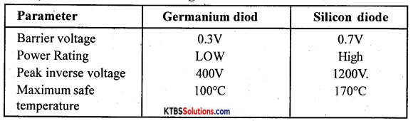
Question 26.
What is etching? Mention any two advantages of PCB.
Answer:
Etching is the process of removing unwanted regions of copper leaving the desired pattern of interconnections.
Advantages of PCB:
- Many components can be assembled in a smaller area.
- Assembling can be done by fully automated machines.
PART-D
Answer any three questions. Each question carries FIVE marks. (3 × 5 = 15)
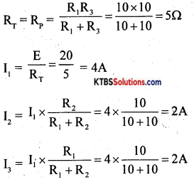
Question 27.
Find the current through 4Ω resistor using superposition theorem.
Answer:
Step 1: E1 alone ON and E2 replaced by a short.
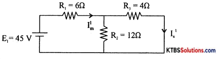
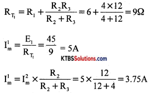
Step 2: E2 alone is ON and E1 replaced by short
RT = R3 + \(\frac{R_{1} R_{2}}{R_{1}+R_{2}}\) = 4 + \(\frac{6 \times 12}{6+12}\) = 8Ω
I”m = \(\frac{\mathrm{E}_{2}}{\mathrm{R}_{\mathrm{T}_{2}}}=\frac{16}{8}\) = 2A
From the principle of superposition, current through 4Ω resistor is I = I’m – I”m
= 3.75 – 2 = 1.75A .
![]()
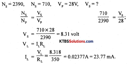
Question 28.
Calculate load current and load voltage in the transformer circuit
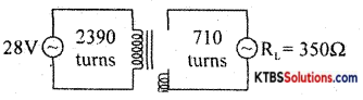
Answer:
Question 29.
For the Zener diode regulator shown, find
(1) load voltage
(2) voltage drop across the series resistor
(3) the current through the diode
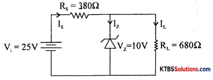
Answer:
Question 30.
A 100pF capacitor in series with a 40Ω resistance is connected to a 110V, 60Hz supply.
(i) Find the current in the circuit.
(ii) What is the phase difference between current and voltage.
Answer:
XC = \(\frac{1}{2 \pi \mathrm{fc}}\) =26.5Ω
Z = \(\sqrt{\mathrm{R}^{2}+\mathrm{X}_{\mathrm{c}}^{2}}\) =48Ω
I = \(\frac{\mathrm{V}}{\mathrm{Z}}\) = 2.29A
tanΦ = \(\frac{X_{C}}{R}=\frac{26.5}{40}\) = 0.6630
Φ = 32.5°
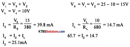
Question 31.
Subtract (16)10 from (22)10 using 2’s complement method.
Answer:
(22)10 = (10110)2
Minuend 10110
Subtrahend 10000
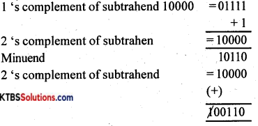
Disregard end around carrying
(110)2
Answer any four questions. Each question carries five (4 × 5 = 20)
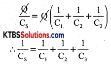
Question 32.
(a) Derive an expression for the effective capacitance of capacitors connected in series
Answer:
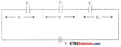
In a series combination, the capacitors are connected end to end. The charge on each capacitor is the same and the emf of the cell equals the sum of voltages across the three resistors.
Consider three capacitors C1, C2, C3 connected in series.
Then V = V1 + V2 + V3.
= \(\frac{\mathrm{Q}}{\mathrm{C}_{1}}+\frac{\mathrm{Q}_{1}}{\mathrm{C}_{2}}+\frac{\mathrm{Q}}{\mathrm{C}_{3}}\)
V = Q\(\left(\frac{1}{C_{1}}+\frac{1}{C_{2}}+\frac{1}{C_{3}}\right)\) ……….(1)
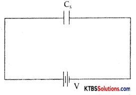
Let the combination be replaced by an equivalent capacitor Cs which has the same effect as the combinations of capacitors. If C is the effective capacitance.
then V = \(\frac{Q}{C_{s}}\) → (2)
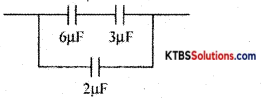
(b) Connect 6μF, 2μF and 3μF capacitors to get effective capacitance of 4μF. (4 + 1)
Answer:
Question 33.
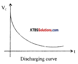
(a) Explain the charging and discharging of a capacitor in an RC circuit when DC is applied.
Answer:
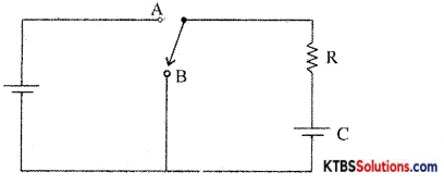
When the switch is in position A, the capacitor gets charged. When the switch is in position B, the capacitor starts getting discharged through resistor R. The voltage across the capacitor decreases and it takes infinite time to get discharged completely. Discharging voltage across the capacitor at times after the switch is in putting in the position B is, V = V0e-t/RC
The time constant can be defined as the time taken by the capacitor to discharge to 3 6.8% of its maximum voltage.
(b) Write the expression for the resonant frequency in LRC circuit. (4 + 1)
Answer:
f = \(\frac{1}{2 \pi \sqrt{\mathrm{LC}}}\)
![]()
Question 34.
(a) Describe iron core inductor.
Answer:
Iron core inductor: In iron core inductors, the coil is wound on a solid laminated iron core. The core is laminated to avoid eddy current losses. A laminated irón core is made up of thin iron laminations pressed together but insulated from each other. These have high inductance values from 1 mH to 1H.

Iron core inductors are used mainly in audio frequency applications and as filters in DC power supplies and in radio and TV receivers.
(b) Mention the factors on which the inductance of an inductor depends upon. (4 + 1)
Answer:
Mutual inductance depends upon
- length of the coil
- number of turns in two coils
- relative permeability of the coil.
Question 35.
(a) What is a passive component?
Answer:
A passive component is a component that dissipates energy and does not supply energy to a circuit.
(b) Explain the working of the loudspeaker.
Answer:
A loudspeaker is a transducer that changes electrical energy into sound waves of varying pressure.
- a coil of wire called a voice coil.
- a permanent magnet
- a cone-shaped piece of stiff paper or cloth called the diaphragm.
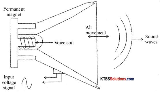
Voice coil is suspended in the strong magnetic field of a circular permanent magnet. The permanent magnet of a speaker provides a steady magnetic field. The two leads of the voice coil are connected with wire to terminals on the speaker frame.
When audio signal current flows through the voice coil, it produces a varying magnetic field in the coil. The varying magnetic field moves the voice coil in and out in accordance with variations in the electrical audio signals. Hence the diaphragm attached to the voice coil vibrates due to which compressions and rarefactions are formed and the sound waves are produced.
Question 36.
Explain the working of the bridge rectifier.
Answer:
The bridge rectifier does not require a centre tap transformer. It uses four diodes D1, D2, D3 and D4 connected in the form of a bridge across the secondary of the transformer.
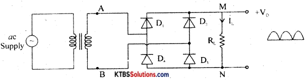
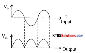
During the positive half cycle of AC input, A is at positive potential and 13 is not at negative potential. D diodes D1 and D3 are forward biased and conduct. The current flows through AD1 MND1B. D2 and D4 do not conduct as they are reverse biased. Thus the positive half cycle of voltage is obtained across the load resistor RL.
During the negative half cycle of AC input, A is at negative potential and B is at positive potential.
Diodes D1 and D4 are forward biased and conduct. Diodes D1 and D1 are reverse biased and do not conduct. Hence current flows along BD2MND4A. Thus a positive half cycle of voltage is developed across the load resistor RL. In both the half cycles, current flows through RL in the same direction from M to N.
Thus varying DC output is obtained across RL.
RMS value of voltage is Vrms = \(\frac{\mathrm{V}_{\mathrm{m}}}{\sqrt{2}}\)
Ripple factor is the ratio of the RMS value of the AC component of the load voltage to the average value of load voltage.
r = Ripple factor = \(\frac{V_{\text {rins }}}{V_{\text {avg }}}=\sqrt{\left(\frac{I_{\mathrm{rms}}}{I_{\mathrm{d}}}\right)^{2}}\) – 1 = 0.48
Efficiency (η) is the ratio of output DC power to the input AC power.
η = \(\frac{\text { DC output power }}{\text { AC input power }}\) r = 0.812 or 81.2%
Question 37.
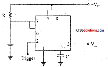
(a) Draw the circuit diagram of an astable multivibrator using IC555.
Answer:
The circuit diagram of the monostable pulse generator is as shown below:
(b) Simplify y = \(\overline{\overline{\mathbf{A B}}+\overline{\mathbf{A}}+\mathbf{A} \mathbf{B}}\)
Answer:
\(\overline{\overline{\mathbf{A B}}+\overline{\mathbf{A}}+\mathbf{A} \mathbf{B}}\) = \(\overline{\overline{\mathrm{AB}} \cdot \mathrm{A} \cdot \mathrm{AB}}\)
= ABA(A̅ + B̅) = AB[A.A̅ + AB̅]
= AB[0 + AB̅] =AB.AB= A.BB̅
= A.0 = 0