Students can Download 1st PUC Electronics Model Question Paper 2 with Answers, Karnataka 1st PUC Electronics Model Question Papers with Answers helps you to revise the complete syllabus.
Karnataka 1st PUC Electronics Model Question Paper 2 with Answers
Time: 3.15 Hours
Max Marks: 70
Note : (i) Question paper contains four parts.
(ii) Part-A is compulsory, Part-D contains two subparts (a) problems (b) essay-type questions.
(iii) Explanation without circuit diagram, wherever necessary, does not carry mark.
PART-A
Answer all questions. Each question carries one mark. (10 × 1 = 10)
Question 1.
What is the charge on a body two which 1020 electrons are added?
Answer:
Q = -ne = – 1020 × 1.6 × 10-19 = 1.6 × 101 = 16C.
Question 2.
Write the expression for power in terms of voltage and resistance.
Answer:
P = \(\frac{\mathrm{V}^{2}}{\mathrm{R}}\)
Question 3.
How much is the AC voltage applied to all household electrical devices?
Answer:
230V.
Question 4.
Which type of impurity is to be added to get electrons as minority charge carriers in a semiconductor.
Answer:
Trivalent impurity like Gaihum.
![]()
Question 5.
Mention SI unit of potential difference.
Answer:
Volt.
Question 6.
Name the regions of the transistor in the decreasing order of their widths.
Answer:
Collector, emitter, base.
Question 7.
Draw the circuit symbol of LED.
Answer:

Question 8.
Mention one application of varactor diode.
Answer:
TV receivers.
Question 9.
Can we get a transistor by joining two diodes back to back?
Answer:
No.
Question 10.
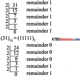
Convert (ACE)16 to binary.
Answer:
(1010 1100 1110)2
PART-B
Answer any five questions. Each question carries two marks. (5 × 2 = 10)
Question 11.
Mention two advantages of a digital thermometer.
Answer:
- Readings are accurate.
- Readings can be taken very quickly.
Question 12.
Find the frequency of an AC of time period 10μS.
Answer:
f = \(\frac{1}{T}=\frac{1}{10 \times 10^{-6}}\) = 105 = 100 × 103Hz = 100kHz.
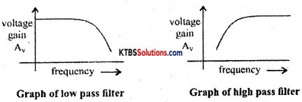
Question 13.
Draw the frequency response curves of low pass and high pass filters.
Answer:
Question 14.
Mention any two applications of a diode.
Answer:
- Rectification
- AM detection
Question 15.
Find β if a is 0.98.
Answer:
β = \(\frac{\alpha}{1-\alpha}=\frac{0.98}{1-0.98}=\frac{0.98}{0.02}=\frac{98}{2}\) = 49
![]()
Question 16.
Mention any two applications of a phototransistor.
Answer:
Phototransistors are used in
- optocouplers
- relay controls.
Question 17.
What is the advantage of2’s complement method of subtraction of binary numbers?
Answer:
By 2’s complement method of subtraction, the same circuit used for addition can be used for Subtraction.
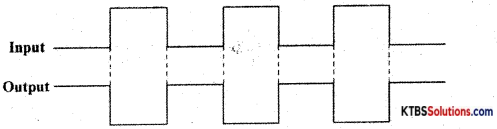
Question 18.
Draw the timing diagram for NOT gate.
Answer:
PART-C
Answer any live questions. Each question carries three marks. (5 × 3 = 15)
Question 19.
Explain the role of electronics in the industries.
Answer:
Industries have used electronics in systems that control production equipment like industríal robots and controlled machine tools. Many risky and life-threatening jobs are now performed by robots. Automation in the industry has reduced human labor, increased safety, and productivity. Electronic fire detectors, burglar alarms, smoke detectors, and CC cameras provide security to industries. Power stations generating electricity are controlled by electronic devices and circuits.
Question 20.
State and explain superposition principle.
Answer:
In any linear bilateral network consisting of two or more independent sources, the resultant current or voltage in any branch is the algebraic sum of the currents or voltages caused by each independent source acting alone, with all other independent sources being replaced by their internal resistances.
Procedure for using Superposition Theorem:
Step 1: Retain the source V1 and replace all other sources with their internal resistances.
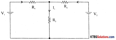
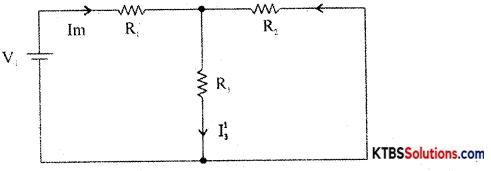
Step 2: Current in various branches and their voltage drops due to V1 alone are determined as follows,
RT1 = R1 + \(\frac{\mathrm{R}_{2} \mathrm{R}_{3}}{\mathrm{R}_{2}+\mathrm{R}_{3}}\)
Im1 = \(\frac{\mathrm{V}_{1}}{\mathrm{R}_{\mathrm{T}_{1}}}\)
I’3 = Im1 × \(\frac{R_{2}}{R_{2}+R_{3}}\) {from branch current formula}
Voltage across R3 = V’3 = I’3 = I”1 = Im2 × \(\frac{R_{1}}{R_{1}+R_{3}}\)
Step 3 : Consider V2 alone and find the currents and voltages as follows:
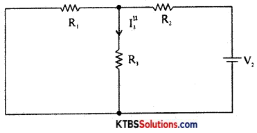
RT2 = R2 + \(\frac{\mathrm{R}_{1} \mathrm{R}_{3}}{\mathrm{R}_{1}+\mathrm{R}_{3}}\)
Im2 = \(\frac{\mathrm{V}_{2}}{\mathrm{R}_{\mathrm{T}_{2}}}\)
I”3 = V2 × \(\frac{\mathrm{R}_{1}}{\mathrm{R}_{1}+\mathrm{R}_{3}}\)
Step 4: Find the algebraic sum of currents and voltage drops in a branch.
I3 = I’3 + I”3; V’3 = I’3R3, V = I”3R3
V3 = V’3 + V”3
![]()
Question 21.
Find the effective resistance between A and B.
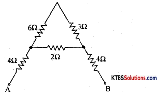
Answer:
RT = \(\frac{R_{1} R_{2}}{R_{1}+R_{2}}=\frac{6 \times 3}{6+3}=\frac{18}{9}\) = 2Ω
Rp = \(\frac{R_{1} R_{2}}{R_{1}+R_{2}}=\frac{2 \times 2}{2+2}\) = 1Ω
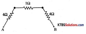
RAB = Rs = R1 + R2 + R3 = 4 + 1 + 4 = 9Ω
Question 22.
What is the self-inductance of a coil? Mention the factors on which self-inductance depends upon.
Answer:
Self-inductance of cold depends on
- number of turns in the coil
- length of the coil
- relative permeability of the coil
- The cross-sectional area of the coil.
Question 23.
Explain the formation of p-type material.
Answer:
A p-type semiconductor is obtained, by adding (doping) trivalent impurity atoms like boron, gallium, indium to a semiconductor. The impurity doping atoms are known as acceptor impurity because they can accept one valence electron from the semiconductor atom.
When trivalent atom-like gallium is added to a silicon crystal, three valence electrons of the gallium atom will form covalent bonds with three valence electrons of three neighboring silicon atoms. The fourth covalent bond remains incomplete and the vacancy in the covalent bond is called a hole. Thus, each gallium atom creates a bole without generating a free electron. Due to the breaking up of few covalent bonds, few electrons and holes are produced.
Thus in p-type semiconductors, holes are majority charge carriers and electrons are the minority charge carriers. Due to the breaking up of few covalent bonds, few electrons and holes are produced.
Thus in p-type semiconductors, holes are majority charge carriers and electrons are the minority charge carriers. Each trivalent atom accepts an electron and hence is called acceptor impurity.
On accepting an electron, the trivalent atom becomes a negative ion. The p-type material is electrically neutral because the number of holes is equal to the sum of a number of electrons and negative ions.

Question 24.
Explain the Zener diode as a line regulator.
Answer:
In a DC power supply. the output voltage should remain almost constant even as the input and load vary.
Voltage regulation is a measure of the ability of a DC source to maintain a constant output voltage, even whén there is variation in the load resistance or input voltage.
Zener diode as a voltage regulator
Zener diode can be used as a voltage regulator to provide a constant output voltage from a source whose voltage may vary.
The two types of voltage regulator are
- Line regulation
- Load regulation.
Load regulation:
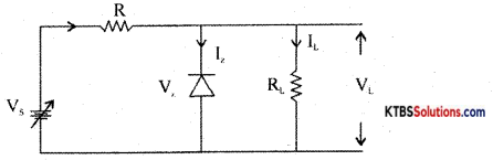
The Zener diode starts conducting only when the source voltage V is greater than Zener breakdown voltage V.
When V is increased from 0V, load current ‘L increases with applied voltage. Current through Zener diode will be zero.
If V is more than V, the Zener diode breaks down and conducts. Increasing the input voltage further increases voltage across the resistor R and voltage across load VL remains constant at V.
Line regulation:
For load regulation, Vs is made greater than Vz. Vs is kept constant and load resistance RL is varied. If RL is decreased, current IL increases and Iz decreases by the same value, but output voltage VL = Vz remains constant.
If RL is increased, IL decreases and Iz increases, but output voltage VL = Vz remains constant.
![]()
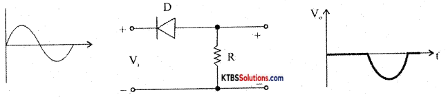
Question 25.
With a circuit diagram, explain the working of the series positive clipper.
Answer:
Question 26.
Mention steps of developing a PCB.
Answer:
PCB layout preparation: PCB layout must be drawn using PC. The complete circuit must be drawn on paper. Prepare computer layout as per circuit diagram using PCB design software.
Draw tracks for connecting one component to the other. Take printout on a white sheet and get the film done on a transparent sheet by filmmakers.
Photoresist: Photoresist film or mask is placed on a copper clad board. UV light is exposed on a copper-clad board covered by photoresist film. UV light does not pass through the photoresist on the tracks. The copper area which is not covered protected by photo-resist is removed during the etching process.
PCB etching process: The etching process is done to remove the unnecessary copper after UV exposure, leaving behind only the desired copper tracks. The PCB is then dipped in fern chloride or hydrochloric acid until unwanted copper is dissolved.
Then the PCB is dipped in acetone to remove the black color giving the PCB a shining attractive look.
PCB Drilling: The components to be attached to PCB can be done only by vias drilling le, by drilling a hole. To make PCB good solderable the surface of the PCB is coated with tin or nickel.
PCB assembling: The electronic components are assembled on the respective holes in the PCB. The component leads are electrically and mechanically fixed to the board with solder.
PART – D
(a) Answer three questions. Each question carries five marks. (3 × 5 = 15)
Question 22.
Using Thevenin’s theorem, find the load current and load voltage of the following circuit.
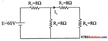
Answer:
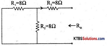
RTh = R3 + \(\frac{R_{1} R_{2}}{R_{1}+R_{2}}\) = 8 + \(\frac{8 \times 8}{8+8}\) = 8 + 4 = 12Ω
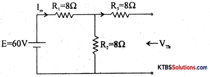
Im = \(\frac{E}{R_{1}+R_{2}}=\frac{60}{8+8}\) = 3.75A
VTh = ImR2 = 3.75 × 8 = 30V
Question 28.
A power line feeds input power at 230V to a step-down transformer with its primary windings having 4000 turns. What should be the number of turns in the secondary in order to get output power at 230V? For efficiency of 0.7, calculate the RMS value of primary current when the RMS value of the secondary current is 5A.
Answer:
XL = 2πfL = 25.14Ω
Xc = \(\frac{1}{2 \pi f c}\) = 53.04Ω
Z = \(\sqrt{\mathrm{R}^{2}+\left(\mathrm{X}_{\mathrm{L}}+\mathrm{X}_{\mathrm{L}}\right)^{2}}=\sqrt{0^{2}+(53.04-25.14)^{2}}\) = 27.9Ω
Im = \(\frac{\mathrm{E}}{\mathrm{Z}}=\frac{230}{27.9}\) = 8.24A
Im = \(\sqrt{2 \mathrm{I}_{\mathrm{rms}}}\) = 1.414 × 8.24
Im = 11.65 A
VL = Im XL = 8.24 × 25.14
VL = 207.15 volt
Vc = ImXc = 8.24 × 53.04
Vc = 437.04 Volt
![]()
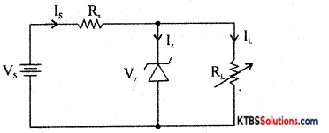
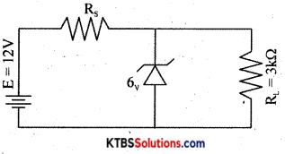
Question 30.
In the circuit shown below, find the value of series resistance Rs, if Zener current is 10mA.
Answer:
VL = Vz = 6V
IL = \(\frac{\mathrm{V}_{\mathrm{Z}}}{\mathrm{R}_{\mathrm{L}}}=\frac{6}{3 \times 10^{3}}\) = 2 × 10⁻³ A = 1mA
Is = Iz + IL
Is = 10 × 10-3 + 2 × 10-3 = 12mA
E = Vs + Vz
12 = Vs + 6
Vs = 6V
R = \(\frac{\mathrm{V}_{\mathrm{s}}}{\mathrm{I}_{\mathrm{S}}}=\frac{6}{12 \times 10^{-3}}=\frac{1000}{2}\) = 500Ω
Question 31.
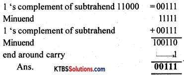
Subtract (24) from (31) using 1 ‘s complement method.
Answer:
(24) = (11000)2
Minuend 11111
Subtrahend 11000
(b) Answer any four questions. Each question carries five marks. (4 × 5 = 20)
Question 32.
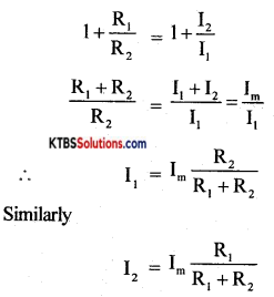
(a) Obtain expressions for branch currents when two resistors are connected in parallel.
Answer:
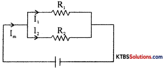
As R1 and R2 are parallel
V1 = V2
I1R1 = I2R2
\(\frac{\mathrm{R}_{1}}{\mathrm{R}_{2}}=\frac{\mathrm{I}_{2}}{\mathrm{I}_{1}}\)
(b) Mention the resistances of closed circuit and open circuit. (3 + 2)
Answer:
Resistance of closed circuit is zero and resistance of the open circuit is infinity.
![]()
Question 33.
(a) Explain the growth and decay of current in an RL circuit.
Answer:
Consider an inductor Land a resistor R connected in series to a cell. When the switch is in position A, the current in the circuit grows exponentially.
The current I at a time after the switch is placed ¡n the position A is t = I0e-(R/L)t, where I0 is the maximum current.
The time constant of RL circuits is the time taken by the current to grow to 63.2% of the maximum value.
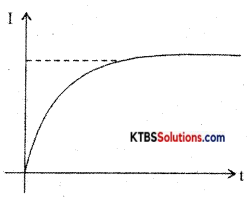
Growth of current in RL circuit
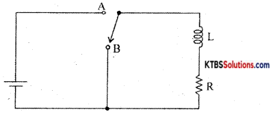
When the switch is in position A, the current in the circuit increases exponentially and reaches a maximum value. When the switch is in position B, the current in the circuit starts decaying exponentially with time.
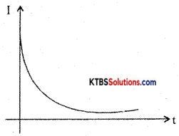
Decay of current
The value of current at a time after the switch is placed in position B is I = I0e(-R/L)t where I0 is the maximum current.
The time constant of the RL circuit is the time taken by the RL circuit for the current to decay to 36.8% of its maximum value.
(b) Find time constant of RC circuit when R = 20kW and C = 0.2mF.
Answer:
T = RC = 20 × 103 × 0.2 × 10-6 = 4 × 10⁻³S = 4ms.
Question 34.
(a) Obtain the expression for the effective capacitance of capacitors connected in series
Answer:
Capacitors are said to be in parallel if they are connected between the same common points.
The voltage across each capacitor in parallel ¡s the same.
Let C1, C2, and C3 be the capacitors connected in parallel.
Let V be the applied voltage across the combination.
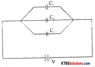
The charge Q from the cell equals the sum of voltages across the capacitors.
Q = Q1 + Q2 + Q3
= C1V1 + C2V2 + C3V3
Q =V(C1 + C2 + C3) → (1)
The equivalent or effective capacitor is a single capacitor that has the same effect as the combination of capacitors.
If Cp is the effective capacitance then
Q = CpV →(2)
From equations (1) and (2).
CpV = V(C1 + C2 + C3)
Cp = C1 + C2 + C3
Hence, when capacitors are connected in series, the effective capacitance is the sum of individual capacitances.
(b) Mention the factors on which the inductance of an inductor depends upon. (4 + 1).
Answer:
- Length of the coil
- Relative permeability of the coil.
- Number of turns of the coil
- The cross-sectional area of the Coil.
![]()
Question 35.
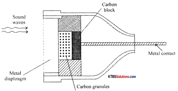
Explain the construction and working of the microphone. ,
Answer:
The microphone is a device that converts sound energy into an electrical signal. It has an insulating button loosely filled with carbon granules. The button ¡s attached to a very thin steel diaphragm.
The diaphragm vibrates when sound waves strike it. Due to vibration, there is variation in the pressure on carbon granules, which changes the resistance of carbon granules in accordance with the pressure of sound waves.
Hence any change in the resistance of carbon granules produces a corresponding change in the current through the circuit. This varying current flowing through the primary coil produces an alternating voltage in the secondary of the transformer.
Question 36.
Explain the working of a half-wave rectifier.
Answer:
Half wave rectifier is a circuit that removes one-half cycle of the AC input and produces a pulsating DC output voltage.
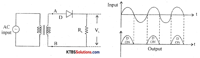
It has diode D in series with a load resistor RL. The AC mains voltage to be rectified ¡s applied to primary of a transformer and voltage induced across secondary is applied to the rectifier.
During the positive half cycle, A is positive and B is negative. The diode is forward biased and conducts and the diode acts as a closed switch, Hence, the positive half cycle of the voltage is developed across the load resistor RL.
During the negative half-cycle, A is negative and LI is positive. The diode is reverse biased and does not conduct as it acts as an open switch. Hence there is no output. The output waveform across RL lias only positive half cycles. Ripple factor is the ratio of the RMS value of (r) the AC component of the load voltage to the average value of load voltage.
r = \(\frac{\text { rms value of AC component }}{\text { value of dccomponent }}\) = 1.21
Rectifier efficiency is the ratio of de output power to ac input power.
η = \(\frac{\text { DC output power }}{\text { AC input power }}\) = 0.406 or 40.6%
Peak inverse voltage is the maximum voltage the diode can withstand when ¡t is reverse biased and is equal to the peak value of the secondary voltage Vm.
Question 37.
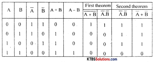
(a) State and explain De-Morgans theorems.
Answer:
First theorem: The complement of a logical sum is equal to the logical product of complements
\(\overline{\mathrm{A}+\mathrm{B}}\) = A̅.B̅
Second theorem: The complement of a logical product is equal to the logical sum of complements.
\(\overline{\mathrm{AB}}\) = A̅ + B̅
Proof:
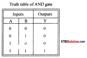
(b) Draw the circuit diagram of the diode AND gate.
Answer:
AND gate is a logic gate that produces a HIGH output only when all its inputs are HIGH.
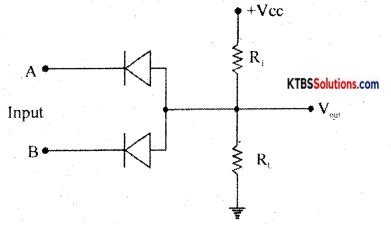
Working:
Case (i) When A = 0, B = 0, both the diodes are forward biased and act like closed switches.
Hence all the applied voltage drops across R1 and the output voltage becomes LOW.
Case (ii) When A = 0, B = 1, diode D1 conducts as it is forward biased and diode D2 does not conduct as it ¡s reverses biased. Hence all the applied voltage drops across R1 and the output voltage becomes LOW.
Case (iii) When A= 1, B = 0, diode D1 does not conduct but D2 conducts being forward biased. Hence all the applied voltage drops across R1 and the output voltage at y becomes LOW.
Case (iv) When A = 1, B = 1 both diodes are reverse biased and do not conduct. No current flows through R and hence no voltage drop across R. Hence output at y becomes HIGH.