Students can Download 1st PUC Electronics Model Question Paper 3 with Answers, Karnataka 1st PUC Electronics Model Question Papers with Answers helps you to revise the complete syllabus.
Karnataka 1st PUC Electronics Model Question Paper 3 with Answers
Time: 3.15 Hours
Max Marks: 70
Note :
- The question paper contains four parts.
- Part-A is compulsory, Part-D contains two subparts (a) problems (b) essay-type questions.
- Explanation without circuit diagram, wherever necessary, does not carry mark.
PART-A
Answer all questions. Each question carries one mark. (10 x 1 = 10)
Question 1.
Who invented the integrated circuit?
Answer:
John Kilby.
Question 2.
What is AC?
Answer:
Alternating Current (AC) is that whose magnitude and direction change continuously and periodically with time.
Question 3.
Write the expression for the electrical power in terms of current and resistance.
Answer:
P = PR.
Question 4.
Why are NPN transistors often used?
Answer:
The mobility of free electrons is faster than the mobility of holes. NPN transistor has electrons as majority charge carriers and hence often used.
![]()
Question 5.
Define SI unit of Potential difference.
Answer:
The potential difference between two points is said to be one volt if 1 joule of work is done in moving one coulomb of charge from one point to another.
Question 6.
What does the arrow mark in the symbol of transistor indicate?
Answer:
The direction of conventional current.
Question 7.
Name the diode that can be used as a voltage regulator.
Answer:
Zener diode.
Question 8.
Draw the symbol of the tunnel diode.
Answer:

Question 9.
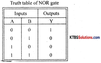
What is NOR gate?
Answer:
NOR gate is a logic circuit whose output is HIGH only when its inputs are LOW.
Question 10.
Convert (110110)2 into a decimal number.
Answer:
(110110)2 = 1 × 25 + 1 × 24 + 0 × 23 + 1 × 22 + 1 × 21 + 0 × 2°
= 32 + 16 + 0 + 4 + 2 + 0
= (54)10.
PART-B
Answer any five questions. Each question carries two marks. (5 × 2 = 10)
Question 11.
What are glucometer and sphygmomanometer?
Answer:
A glucometer measures blood sugar and a sphygmomanometer measures blood pressure.
Question 12.
Find the time period of AC whose frequency is 10kHZ.
Answer:
T = \(\frac{1}{\mathbf{f}}=\frac{1}{10 \times 10^{3}}\) = 0.1 × 10⁻³S = 0.1 ms.
Question 13.
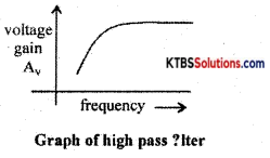
What is an RC high pass filter? Draw its frequency response curve.
Answer:
RC high pass filter is a circuit that passes all the frequencies above the cutoff frequency.
![]()
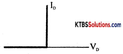
Question 14.
What is an ideal diode? Draw its V-l characteristics.
Answer:
An ideal diode is a diode that acts as a closed switch when forward biased and acts as an open switch when reversing biased.
Question 15.
If β of a transistor is 200, find its α
Answer:
α = \(\frac{\beta}{\beta+1}=\frac{200}{200+1}=\frac{200}{201}\) = 0.995
Question 16.
Convert (6796), into hexadecimal.
Answer:
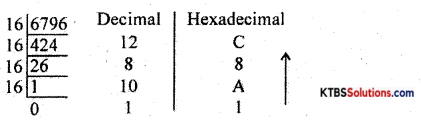
(6796)10 = (1A8C)16
Question 17.
Mention any two applications of Schottky diode.
Answer:
- Detector circuits
- Radar systems.
Question 18.
What are the radix of a number system and mention the radix of the hexadecimal number system?
Answer:
Radix is the number of digits used in the number system.
The Radix of the hexadecimal number system is 16.
PART-C
Answer any five questions. Each question carries three marks. (5 x 3 = 15)
Question 19.
Mention three advantages of E-mail.
Answer:
- E-mail messages reach the destination within minutes.
- E-mail can be used to transfer letters, graphics, recorded audio, and video documents.
- E-mail is highly reliable.
Question 20.
State and explain superposition theorem.
Answer:
In any linear bull era network consisting of two or more independent sources, the resultant current or voltage in any branch is the algebraic sum of the currents or voltages caused by each independent source acting alone, with all other independent sources being replaced by their internal resistances.
Procedure for using Superposition Theorem:
Step 1: Retain the source V1 and replace all other sources with their internal resistances.
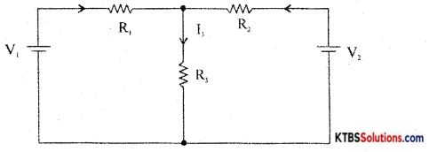
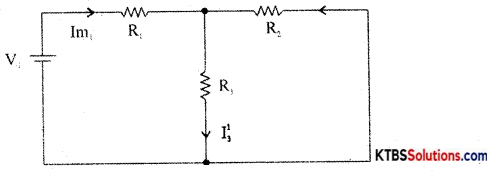
Step 2: Current in various branches and their voltage drops due to V1 alone are determined as follows,
RT1 = R1 + \(\frac{\mathrm{R}_{2} \mathrm{R}_{3}}{\mathrm{R}_{2}+\mathrm{R}_{3}}\)
Im1 = \(\frac{\mathrm{V}_{1}}{\mathrm{R}_{\mathrm{T}_{1}}}\)
I’3 = Im1 × \(\frac{R_{2}}{R_{2}+R_{3}}\) {from branch current formula}
Voltage across R3 = V’3 = I’3 = I”1 = Im2 × \(\frac{R_{1}}{R_{1}+R_{3}}\)
Step 3 : Consider V2 alone and find the currents and voltages as follows:
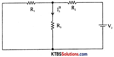
RT2 = R2 + \(\frac{\mathrm{R}_{1} \mathrm{R}_{3}}{\mathrm{R}_{1}+\mathrm{R}_{3}}\)
Im2 = \(\frac{\mathrm{V}_{2}}{\mathrm{R}_{\mathrm{T}_{2}}}\)
I”3 = V2 × \(\frac{\mathrm{R}_{1}}{\mathrm{R}_{1}+\mathrm{R}_{3}}\)
Step 4: Find the algebraic sum of currents and voltage drops in a branch.
I3 = I’3 + I”3; V’3 = I’3R3, V = I”3R3
V3 = V’3 + V”3
Question 21.
What are open and closed circuits? Mention their resistances.
Answer:
(i) Zero
(ii) Infinity.
Question 22.
Explain the wire wound resistors.
Answer:
Wire wound resistor is made by winding a wire of known length on a hollow porcelain tube. Eureka wire, an alloy of 60% nickel and 40% copper, is used as a resistance wire. Tinned copper leads are attached to the ends of the winding for connection.
The entire assembly is covered with a protective insulation coating of porcelain. The length, thickness, and specific resistivity of the resistance wire determine the resistance value. Their resistance varies from 1 Ω to 1000Ω. They are available with a power rating from 5W to 100W. Wire wound resistors have good stability, reliability, and high power ratings. The resistance value and the power ratings are printed on the body of the resistance. These resistors are used in audio frequency applications.
Question 23.
Explain the formation of p-type material.
Answer:
A p-type semiconductor is obtained, by adding (doping) trivalent impurity atoms like boron, gallium, indium to a semiconductor. The impurity doping atoms are known as acceptor impurity because they can accept one valence electron from the semiconductor atom.
When trivalent atom-like gallium is added to a silicon crystal, three valence electrons of the gallium atom will form covalent bonds with three valence electrons of three neighboring silicon atoms. The fourth covalent bond remains incomplete and the vacancy in the covalent bond is called a hole. Thus, each gallium atom creates a hole without generating a free electron. Due to the breaking up of few covalent bonds, few electrons and holes are produced.
Thus in p-type semiconductors, holes are majority charge carriers and electrons are the minority charge carriers. Due to breaking up few covalent bonds, few electrons and holes are produced.
Thus in p-type semiconductors, holes are majority charge carriers and electrons are the minority charge carriers. Each trivalent atom accepts an electron and hence is called acceptor impurity.
On accepting an electron, the trivalent atom becomes a negative ion. The p-type material is electrically neutral because the number of holes is equal to the sum of a number of electrons and negative ions.

![]()
Question 24.
Explain the working of the bridge rectifier.
Answer:
The bridge rectifier does not require a center tap transformer. It uses four diodes D1, D2, D3, and D4 connected in the form of a bridge across the secondary of the transformer.
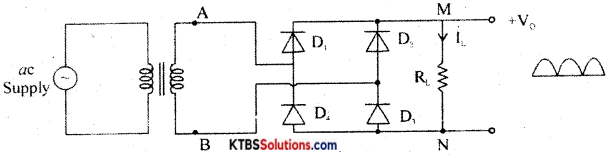
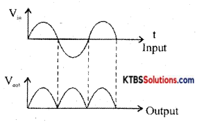
During the positive half cycle of AC input, A is at positive potential and 13 is not at negative potential. D diodes D1 and D3 are forward biased and conduct. The current flows through AD1 MND1B. D2 and D4 do not conduct as they are reverse biased. Thus the positive half cycle of voltage is obtained across the load resistor RL.
During the negative half cycle of AC input, A is at negative potential and B is at positive potential.
Diodes D1 and D4 are forward biased and conduct. Diodes D1 and D1 are reverse biased and do not conduct. Hence current flows along BD2MND4A. Thus a positive half cycle of voltage is developed across the load resistor RL. In both the half cycles, current flows through RL in the same direction from M to N.
Thus varying DC output is obtained across RL.
RMS value of voltage is Vrms = \(\frac{\mathrm{V}_{\mathrm{m}}}{\sqrt{2}}\)
Ripple factor is the ratio of the RMS value of the AC component of the load voltage to the average value of load voltage.
r = Ripple factor = \(\frac{V_{\text {rins }}}{V_{\text {avg }}}=\sqrt{\left(\frac{I_{\mathrm{rms}}}{I_{\mathrm{d}}}\right)^{2}}\) – 1 = 0.48
Efficiency (η) is the ratio of output DC power to the input AC power.
η = \(\frac{\text { DC output power }}{\text { AC input power }}\) r = 0.812 or 81.2%
Question 25.
If IB = 10μA, Ic = 5mA, find α and IE.
Answer:
IE= IB + IC = 10 × 10-6 + 5 × 10-3 = 10-3 (0.01 + 5) = 5.01 mA.
α = \(\frac{I_{C}}{I_{E}}=\frac{5}{5.01}\) = 0.99
Question 26.
What is a datasheet? Mention any two pieces of information given by a data sheet?
Answer:
- Product number and name
- Pin connection diagram.
- Absolute minimum, maximum ratings.
- Recommended operating conditions.
- Input/output waveshape diagrams.
PART-D
(a) Answer any three questions. Each question carries five marks. (3 × 5 = 15)
Question 27.
Find the currents in the following circuit using Kirchoff’s laws.
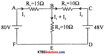
Answer:
Apply KVL to the loop ABEFA,
15I1 + 10(I1 + I2)= 80
25I1 + 10I2 = 80
5I1+ 2I2 = 16 ……….(I)
Apply KVL to the loop CBEDB,
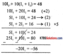
I1 = 2.8A
5I1 + 2I2 = 16
5 × 2.8 + 2I1 = 16
I2 = \(\frac{16-14}{2}\) = 1
I2 = 1A
I1 + I2 = 2.8 + 1 = 3.8A
![]()
Question 28.
An AC of 125V is applied to the primary transformer of power efficiency 60% so that the secondary current is 500mA. If the loss of power in the score is low, calculate primary current, secondary voltage, output power, and input power.
Answer:
Pi = P0 + PL, η = \(\frac{P_{0}}{P_{i}}=\frac{P_{0}}{P_{0}+P_{L}}\)
P0 = \(\frac{\mathrm{P}_{\mathrm{L}}}{\frac{1}{\eta}-1}\) = 15W
P0 = IS IVS
15 = 500 × 10-3 × Vs
Vs = 30V
Pi = P0 + PL
Pi = 25W
Pi = VpIp
25 = 125 × Ip
Ip = 0.2A
Question 29.
A coil of resistance 100, an inductor of 0.511, and a capacitor of ISJ.!F are connected in series with a 200V, 50Hz AC source. Calculate the current in the circuit.
Answer:
XC = \(\frac{1}{2 \pi \mathrm{fc}}\) = 212.2
XL = 2πfL = 157.1
Z = \(\sqrt{R^{2}+\left(X_{L}-X_{C}\right)^{2}}=\sqrt{(100)^{2}+(157.1-212.2)^{2}}\) = 114.1
I = \(\frac{\mathrm{V}}{\mathrm{Z}}=\frac{100}{114.1}\) = 1.725A
Question 30.
For the following circuit, find
(a) load voltage
(b) VRS
(c) current through the diode
Answer:
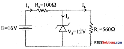
RL(min) = \(\frac{\mathrm{R}_{\mathrm{S}} \mathrm{V}_{\mathrm{z}}}{\mathrm{V}_{\mathrm{i}}-\mathrm{V}_{\mathrm{z}}}=\frac{100 \times 12}{16-12}\) = 300W
As RL > RL(min), Zener diode is ON
E = Vs + Vz
16 = Vs + 12
Vs = 4V
Is = \(\frac{V_{s}}{R_{s}}=\frac{4}{100}\) = 40mA
IL = \(\frac{\mathrm{V}_{\mathrm{L}}}{\mathrm{R}_{\mathrm{L}}}=\frac{12}{560}\) = 21.4mA
Is = Iz + IL
40 = Iz 21.4
Iz = 18.6mA
![]()
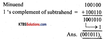
Question 31.
Subtract (25)2 from (36)2 using 1 ‘s complement method.
Answer:
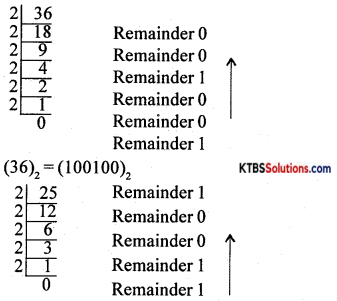
(25)10= (11001)2
Minuend 100100
Subtrahend 011001
(b) Answer any four questions. Each question carries five marks. (4 x 5 = 20)
Question 32.
(a) Define the following for an AC
(i) Frequency
Answer:
The frequency of AC is the number of AC cycles completed in one second.
(ii) Time period
Answer:
The time period of AC is the time taken to complete one cycle.
(iii) Peak value
Answer:
The peak value of AC is the maximum voltage or current of the ac in its one of half cycles.
(iv) RMS value
Answer:
RMS value of ac is the equivalent steady DC value which gives the same heating effect as the same rate in a given resistor.
(v) Average value
Answer:
The peak to the peak value of AC is the maximum value attained in both positive and negative half cycles of AC.
Question 33.
Derive the expression for the resonant frequency of a series resonant circuit.
Answer:
Consider an AC circuit consisting of inductance (L), capacitor C and a resistance R connected in series to an AC source. Let the instantaneous voltage of the ac source be
v = Vm sin wt
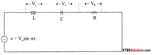
Let VL, VR, V be the voltages across the inductor, Resistor, and capacitor.
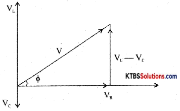
Result voltage V = \(\sqrt{V_{R^{2}}+\left(V_{L}-V_{C}\right)^{2}}\)
= \(\sqrt{I^{2} R^{2}+\left(I X_{L}-I X_{C}\right)^{2}}\)
= \(\sqrt{I^{2}\left[R^{2}+\left(X_{L}-X_{C}\right)^{2}\right]}\) = I\(\sqrt{R^{2}+\left(X_{L}-X_{C}\right)^{2}}\)
As the frequency of AC source is increased, the capacitive reactance of the capacitor decreases and .inductive reactance of the .inductnr increases . The values of X1 and XC will be same at resonance frequency fr.
XL = XC
2πfr L = \(\frac{1}{2 \pi \mathrm{f}_{\mathrm{r}} \mathrm{C}}\)
4π2fr2 LC = 1
fr2 = \(\frac{1}{4 \pi^{2} L C}\), fr = \(\frac{1}{2 \pi \sqrt{\mathrm{LC}}}\)
The current in RLC circuit will be maximum at resonance the variation of current with frequency is as shown below:
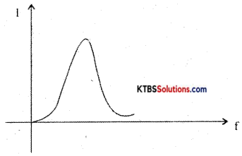
Question 34.
(a) Explain the principle of a capacitor.
Ans.
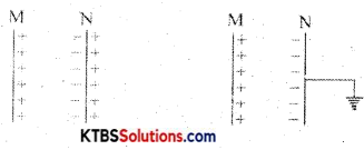
Consider two metal plates M and N separated by a small distance. Let the inner surface of metal plate M be positively charged. Then due to electrostatic induction, an equal and opposite negative, the charge is induced on the inner surface of metal plate N, and an equal positive charge is induced on the outer surface of plate N. The negative charge on N tries to decrease the potential on M and positive charge on N tries to increase the potential on M. As the negative charges on plate N are nearer to plate M, it has a greater effect on plate N.
Hence, there is a net decrease in potential on M and thus the capacitance of the capacitor increases. If the outer surface of plate N is grounded (or connected to earth), the charges on the outer surface of plate N are neutralized. Due to negative charges only on plate N, the potential of plate M is greatly reduced. Hence the capacitance of plate M increases. When a grounded conductor is placed near a charged conductor with a dielectric medium in between, the capacitance of the system increases.
The capacitance of the capacitor can be increased by
- reducing the distance between the plates.
- placing the medium of a high dielectric constant between the plates of the capacitor.
(b) Mention any two methods of increasing the capacitance of a capacitor
Answer:
- An increasing area of plates
- Decreasing the distance between plates.
- Using a medium of high dielectric constant.
![]()
Question 35.
(a) Explain the high pass filter with the circuit.
Answer:
A high pass filter passes all high frequencies above cut-off and rejects the lower frequencies.
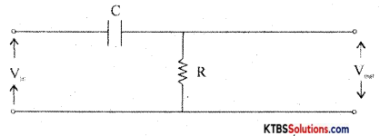
At low frequencies, capacitor acts as open circuit (∴ X = \(\frac{1}{2 \pi \mathrm{RC}}\) = HIGH) At high frequencies, the capacitor acts as a short circuit. Hence all the input appears the output resistor. The cut off frequency, fc = \(\frac{1}{2 \pi \mathrm{RC}}\)
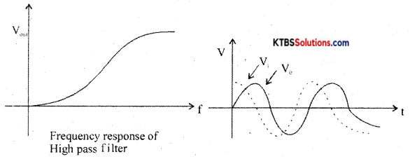
As the output voltage leads the input voltage, the high pass filter is also called a lead network.
(b) What is the quality factor of the RLC circuit?
Answer:
The quality factor of a circuit is the ratio of resonant frequency to the bandwidth.
Question 35.
(a) Explain the working of center tap full-wave rectifier,
(b) Define the ripple factor.
Answer:
A full-wave rectifier is a circuit that converts the entire AC input cycle into varying DC output.
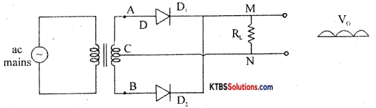
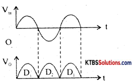
During the positive half cycle of AC input, A is at positive potential and 13 is not at negative potential. D diodes D1 and D3 are forward biased and conduct. The current flows through AD1 MND1B. D2 and D4 do not conduct as they are reverse biased. Thus the positive half cycle of voltage is obtained across the load resistor RL.
During the negative half cycle of AC input, A is at negative potential and B is at positive potential.
Diodes D1 and D4 are forward biased and conduct. Diodes D1 and D1 are reverse biased and do not conduct. Hence current flows along BD2MND4A. Thus a positive half cycle of voltage is developed across the load resistor RL. In both the half cycles, current flows through RL in the same direction from M to N.
Thus varying DC output is obtained across RL.
RMS value of voltage is Vrms = \(\frac{\mathrm{V}_{\mathrm{m}}}{\sqrt{2}}\)
Ripple factor is the ratio of the RMS value of the AC component of the load voltage to the average value of load voltage.
r = Ripple factor = \(\frac{V_{\text {rins }}}{V_{\text {avg }}}=\sqrt{\left(\frac{I_{\mathrm{rms}}}{I_{\mathrm{d}}}\right)^{2}}\) – 1 = 0.48
Efficiency (η) is the ratio of output DC power to the input AC power.
η = \(\frac{\text { DC output power }}{\text { AC input power }}\) r = 0.812 or 81.2%
Question 37.
Describe the working of the DTL NOR gate.
Answer:
NOR gate ¡s a logic circuit whose output is HIGH only when both its inputs are LOW
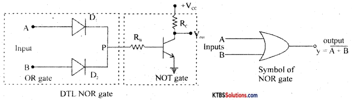
Diodes D1 and D2 form OR gates and the transistor act as NOT gate.
Case (I) When A = O, B = O, the diodes are not forward biased and they do not conduct. Hence voltage P is zero. This zero voltage makes the transistor go to cut-off condition and therefore output is HIGH.
Case (ii) When A= O, B = 1, D1 does not conduct but D2 conducts. Hence voltage at P is +Vcc and drives transistor to saturation and output becomes LOW.
Case (iii) When A = 1, B = O, D1 conducts and D2 does not conduct. Hence voltage at P is +Vcc and this makes the transistor Q go to saturation. Hence output becomes LOW.
Case (iv) When A = 1, B = 1, both diodes conduct as they are forward biased. Then voltage at P is +Vcc and the transistor is driven to saturation. The output at the collector becomes LOW.