Students can Download 1st PUC Electronics Previous Year Question Paper March 2014 (North), Karnataka 1st PUC Electronics Model Question Papers with Answers helps you to revise the complete syllabus.
Karnataka 1st PUC Electronics Previous Year Question Paper March 2014 (North)
Time: 3.15 Hours
Max Marks: 70
Note:
- The question paper contains four parts.
- Part – A is compulsory, Part – D contains two subparts (a) problems (b) essay-type questions.
- Draw the circuit diagram, wherever necessary.
PART – A
Answer all questions. Each question carries one mark. (10 × 1 = 10)
Question 1.
Who invented the transistor?
Answer:
William Shockley, John Bardeen, Walter Brattain.
Question 2.
Give the expression for electric current in terms of charge.
Answer:
I = Electric current = \(\frac{\text { charge }}{\text { time }}\)
Question 3.
Mention the device used to measure blood pressure.
Answer:
Sphygmomanometer.
Question 4.
Mention the color code for a resistor of resistance 390Ω.
Answer:
Orange White Brown.
![]()
Question 5.
What is the phase difference between current and voltage in a series LCR circuit at resonance?
Answer:
Zero.
Question 6.
Mention any one type of acceptor impurity.
Answer:
Gallium.
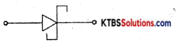
Question 7.
Draw the symbol of a Schottky diode.
Answer:
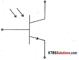
Question 8.
What does an arrow in the circuit symbol of a transistor indicate?
Answer:
The arrow mark in the symbol of a transistor indicates the direction of flow of conventional current.
![]()
Question 9.
Convert (4DD)16 to binary.
Answer:
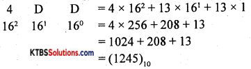
Question 10.
Name the type of capacitor having polarity.
Answer:
Electrolytic capacitor.
PART-B
Answer any five questions. Each question carries two marks. (5 x 2 = 10)
Question 11.
Write any two advantages of E-mail.
Answer:
- E-mail is very fast
- E-mail is economical
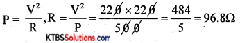
Question 12.
The specifications of an iron box are labeled as 220V, 500W. Calculate the resistance of the iron box.
Answer:
V = 220V, P = 500W
Question 13.
Mention any two applications of an oscilloscope.
Answer:
An oscilloscope is used to
- measure AC/DC voltage
- measure time period and frequency of AC
Question 14.
Define the time constant of the LR circuit. Write an expression for it.
Answer:
The time constant of the RL circuit is the time taken by the current to grow to 63.2% of the maximum value.
Time constant T = \(\frac{\mathrm{L}}{\mathrm{R}}\)
![]()
Question 15.
Define ideal diode. Draw its V-I characteristics.
Answer:
An ideal diode is a diode that conducts with zero resistance (perfect conductor) when forward biased and offers infinite resistance (perfect insulator) when reversing biased.
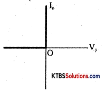
V-I characteristics of Ideal Diode
Question 16.
What is a phototransistor? Draw its symbol.
Answer:
The phototransistor is a transistor that is sensitive to incident light on it.
Symbol of phototransistor
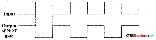
Question 17.
What is a timing diagram? Sketch the timing diagram of NOT gate.
Answer:
Timing diagram is the pictorial representation of input and output states of a logic circuit.
Question 18.
Prove that A + ĀB = A + B.
Answer:
LHS = A + ĀB
= A.1 + ĀB {QA=A.l}
= A(1 + B) + ĀB {Ql = l + B}
= A + AB + ĀB
= A + B(A+ Ā)
= A + B. 1 {QA + Ā = 1}
= A + B
= RHS
PART-C
Answer any five questions. Each question carries three marks. (5 x 3 = 15)
Question 19.
Derive an expression for the effective resistance of two resistors connected in parallel.
Answer:
Consider two resistors R1 and R2 connected in parallel between the same two common points.
In parallel combination, the voltage across each resistor is the same.
Let I1 and I2 be the currents through the resistors R1 and R2.
The current from the cell equals the sum of the currents through the two resistors, i.e.,
I = I1 + I2 = \(\frac{V}{R_{1}}+\frac{V}{R_{2}}\) = V\(\left(\frac{1}{R_{1}}+\frac{1}{R_{2}}\right)\) → (1)
Equivalent or effective resistor Rp is a single resistor that has the same effect as a tile parallel combination. If Rp is the effective resistor, then I = \(\frac{\mathrm{V}}{\mathrm{Rp}}\) → (2)
From equation (1) and (2)
\(\frac{\mathrm{V}}{\mathrm{Rp}}\) = V\(\left(\frac{1}{R_{1}}+\frac{1}{R_{2}}\right)\)
\(\frac{1}{\mathrm{Rp}}=\frac{1}{\mathrm{R}_{1}}+\frac{1}{\mathrm{R}_{2}}\)
Hence, the reciprocal of effective resistance of a number of resistors in parallel is sum 0f the reciprocals of the individual resistances.
![]()
Question 20.
Define the following terms with respect to an AC.
(a) Cycle
Answer:
The time period of AC is the time taken to complete one cycle.
(b) Frequency
Answer:
The frequency of AC is the number of AC cycles completed in one second.
(c) Peak value
Answer:
The peak value of AC is the maximum voltage or current of the ac in its one of half cycles.
Question 22.
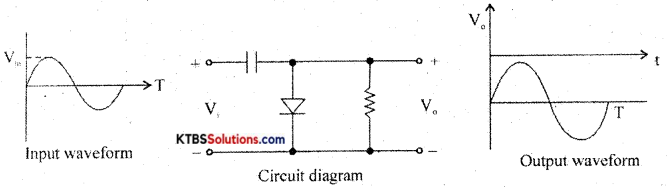
Explain the filtering action of a low pass filter and draw its frequency response.
Answer:
The low pass filter passes all the low frequencies below a cutoff frequency and stops or attenuates the higher frequencies.
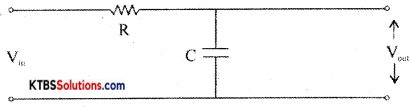
![]()
The input is applied across the RC circuit and the output is taken across the capacitor.
At low frequencies, the capacitive reactance X = \(\frac{1}{2 \pi \mathrm{fc}}\) is high and hence entire input voltage appears across the output. At high frequencies, the capacitor offers very low reactance and acts as a short circuit and hence output becomes Zero. The cut off frequency fc = \(\frac{1}{2 \pi R c}\)
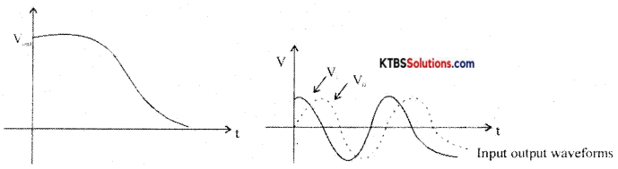
Since the output voltage lags the input voltage, a low pass filter is also called a lag network.
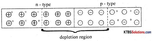
Question 23.
How is the depletion region formed in a p-n junction?
Answer:
A p-n junction is formed when one side of a pure semiconductor crystal is doped with a trivalent impurity and the other side with a pentavalent impurity.
The n-type material has electrons as majority charge carriers and holes as minority charge carriers. The p-type material has holes as majority charge carriers and electrons as minority charge carriers. Due to this, there is a concentration gradient across the junction and electrons move from n-type to p-type whereas holes move from p-type to n-type region. The transfer of electrons and holes across the junction is known as diffusion. The recombination of electrons and holes makes the region near the p-n junction depleted of electrons and holes.
The depletion region is the region near the p-n junction which is depleted of mobile charge carriers namely electrons and holes.
The small potential difference developed across the p-n junction due to immobile positive and negative ions is called barrier potential. The barrier voltage is 0.3V for Germanium and 0.7V for silicon. The barrier potential stops the diffusion of charge carriers across the p-n junction.
![]()
Question 24.
Explain with a circuit diagram the action of positive clamper.
Answer:
A negative clamper is a circuit that clamps the negative peak of a signal to a desired de level.
Question 25.
Explain the working of an n-p-n transistor.
Answer:
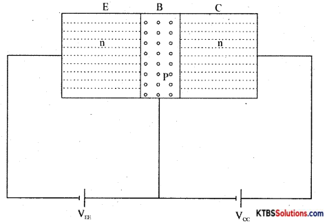
The emitter-base junction is forward biased by power supply VEE and the collector-base junction is reverse biased by the power supply VCC.
The negative terminal of VEE repels the majority charge carriers electrons in the n-type emitter towards the base region. When VEE is greater than the barrier potential of the emitter-base junction the electrons from the emitter region move to the p-type base region. This forms the emitter current IE.
The base ¡s thin and has only a few electrons. Hence only a few electrons and holes recombine and this forms the base current IE. The remaining free electrons in the base region move to the collector region attracted by the +Vcc. They move through the collector region into +Vcc, This forms collector current Ic.
The relation connecting the currents in the transistor is IE = IB + IC
Question 26.
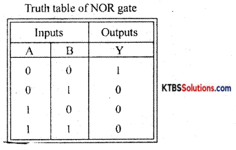
Explain the working of two input DTL NOR gates.
Answer:
NOR gate ¡s a logic circuit whose output is HIGH only when both its inputs are LOW
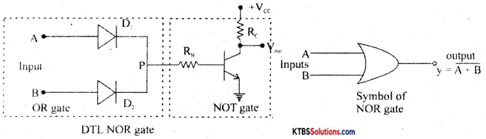
Diodes D1 and D2 form OR gates and the transistor act as NOT gate.
Case (I) When A = O, B = O, the diodes are not forward biased and they do not conduct.
Hence voltage P is zero. This zero voltage makes the transistor go to cut-off condition and therefore output is HIGH.
Case (ii) When A= O, B 1, D does not conduct but D2 conducts. Hence voltage at P is +Vcc and it drives the transistor to saturation and output becomes LOW.
Case (iii) When A = 1, B = O, D1 conducts and D2 does not conduct. Hence voltage at P is +Vcc and this makes the transistor Q go to saturation. Hence output becomes LOW.
Case (iv) When A = 1, B = 1, both diodes conduct as they are forward biased. Then voltage at P is +Vcc and the transistor ¡s driven to saturation. The output at the collector becomes LOW.
![]()
PART-D
(a) Answer any three of the following. (3 x 5 = 15)
Question 27.
Calculate the current through 8Ω resistors using superposition theorem.
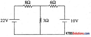
Answer:
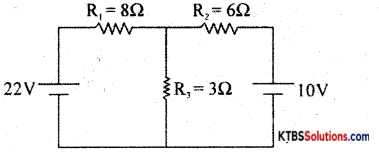
(i) 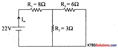
RT = R1 + \(\frac{\mathrm{R}_{2} \mathrm{R}_{3}}{\mathrm{R}_{2}+\mathrm{R}_{3}}\) = 8 + \(\frac{6 \times 3}{6+2}\) = 8 + 2 = 10
Im = \(\frac{\mathrm{V}}{\mathrm{R}_{\mathrm{T}}}=\frac{22}{10}\) = 2.2A
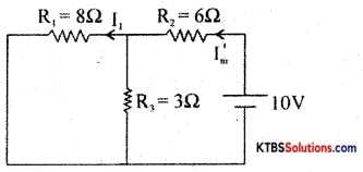
RT = R2 + \(\frac{R_{1} R_{3}}{R_{1}+R_{3}}\) = 6 + \(\frac{8 \times 3}{8+3}\) = 6 + \(\frac{24}{11}\) = 6 + 2.18 = 8.81Ω
I’m = \(\)
From branch current formula,
I1 = Im × \(\frac{R_{3}}{R_{1}+R_{3}}\) = 1.22 × \(\frac{3}{3+8}\) = \(\frac{1.22 \times 3}{11}\) = 0.33A
From principle of superposition..currcnt through 8Ω resistor is Im – I1 = 2.2 – 0.33 = 1.87A
Question 28.
Find the load current using Thevenin’s theorem.
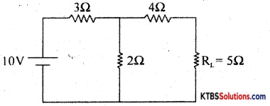
Answer:
To find RTh
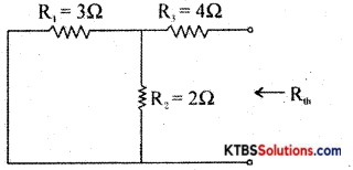
RTh = 4 + 3 ∥ 2 = 4 + \(\frac{6}{5}\) = 5.2Ω
To find VTh
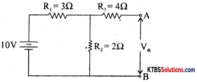
VTh = Voltageacross R2 = \(\frac{\mathrm{VR}_{2}}{\mathrm{R}_{1}+\mathrm{R}_{2}}\) = 10 × \(\frac{2}{3+2}\) = 4V
Thevenin’s equivalent circuit
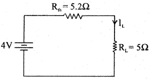
IL = \(\frac{\mathrm{V}_{\mathrm{Th}}}{\mathrm{R}_{\mathrm{L}}+\mathrm{R}_{\mathrm{Th}}}=\frac{4}{5.2+5}=\frac{4}{10.2}\) = 0.39A
![]()
Question 29.
A series circuit with R = 1000, L = 10mH and C = 10pF is connected to a 220V, 50HzAC source. Calculate the total impedance, circuit current, and resonant frequency of the LCR circuit.
Answer:
R = 1000, L = 10mH = 10 × 10-3 H5C = 10μF = 10 × 10-6F
V = 220V, f = 50Hz.
XL = 2πfL = 2(3.14) (50) (10 × 10-3) = 3140 × 10-3 Ω = 3.14Ω
Z = \(\sqrt{\mathrm{R}^{2}+\mathrm{X}_{\mathrm{L}}^{2}}=\sqrt{(100)^{2}+(3.14)^{2}}=\sqrt{10,000+9.765}\) = 100.04Ω
I = \(\frac{\mathrm{V}}{\mathrm{Z}}=\frac{220}{100.04}\) = 2.19 A
fc = \(\frac{1}{2 \pi \sqrt{L C}}=\frac{1}{2 \times 3.14 \sqrt{10 \times 10^{-3} \times 10 \times 10^{-6}}}\)
\(\frac{1}{6.28 \times \sqrt{10 \times 10^{-8}}}=\frac{1}{6.28 \times \sqrt{10} \times 10^{-4}}=\frac{10,000}{6.28 \times 3.16}\)
fr = 503.9 Hz
Question 30.
A center-tapped transformer has a 220V primary winding and a secondary winding rated at 9-0-9 and is used in a full-wave rectifier circuit with a load of 100Ω. What is the de output voltage, decurrent, and the PIV rating required for diodes?
Answer:
Vm = \(\sqrt{2}\) × Vrms = \(\sqrt{2}\) × 9 = 12.7 volt
RL = 100W
Vdc = \(\frac{2 \mathrm{~V}_{\mathrm{m}}}{\pi}=\frac{2 \times 12.7}{3.14}\) = 8.08 volt
Idc = \(\frac{2 \mathrm{I}_{\mathrm{m}}}{\pi}=\frac{2 \mathrm{~V}_{\mathrm{m}}}{\pi \mathrm{R}_{\mathrm{L}}}=\frac{2 \times 12.7}{3.14 \times 100}\) = 0.08A
PIV of the diodes. = 2V = 2 × \(\sqrt{2}\) Vrms = 2 × 1.414 × 9 = 25.4 volt
Question 31.
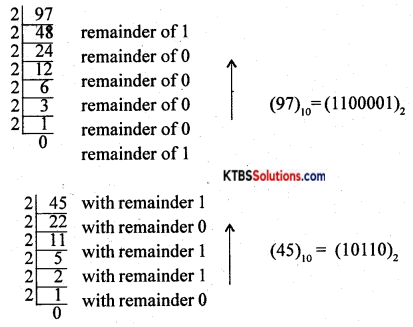
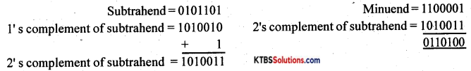
(a) Subtract (45)10 from (97)10 using 2’s complement method.
(b) Simplify: Y = \(\overline{\overline{\mathbf{A}} \mathbf{B}+\mathbf{A} \overline{\mathbf{B}}}\)
Answer:
= (A+B̅).(A̅+B)
= AA̅ + AB + B̅A + B̅B
= 0 + AB + A̅B̅ + 0
= AB + A̅B̅
= A + A. 1
= A + A
= A.
(b) Answer any four questions. (4 × 5 = 20)
Question 32.
(a) State and explain Kirchoff’s voltage law.
Answer:
Consider two resistors R1 and R2 connected in series to a cell of emf E. In a series combination, the resistors are connected end to end and the same current flows through each of them.
The emf of the cell equals voltage drops across each of the resistors
E = V1 + V2 = IR1 + IR2 {from ohms Iaw}
E = I(R1 + R2) → (1)
The effective or equivalent resistor is a single resistor that has the same effect as a combination of resistors. If R5. is the effective resistance, E = IR5 — (2)
From the equations (1) and (2), IR = I (R1 + R2)
∴ Rs = R1 + R2
∴ The effective resistance of resistors in series ¡n sum of the individual resistances.
(b) Mention any two limitations of Ohm’s law.
Answer:
- Like charges repel and unlike charges attract each other.
- Charges can neither be created nor be destroyed.
- Charges take only integral values.
- Charges on a body are not affected by the motion of the body.
- Charges always reside only on the outer surface of a conductor only.
Question 33.
(a) What is a transformer? Explain the construction and working of an AF transformer.
(b) Mention any two specifications of LED.
Answer:
(a) Transformer is a device used to step up or step down ac voltages. A transformer works between frequencies 20Hz to 20kHz and is used in audio amplifier circuits. Centre tapped secondary winding can be used to select different turns ratio.
Phase splitting transformers with center-tapped secondary windings can be used to provide two out of phase signals.
These are used to couple microphone to an amplifier and to couple amplifier to a loudspeaker,
(b) Diameter, color, quality.
![]()
Question 34.
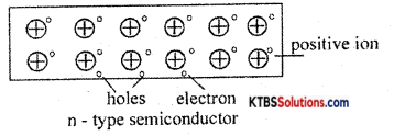
(a) Explain how N-type semiconductors are formed.
Answer:
n-type semiconductors are semiconductors that are doped with pentavalent impurities like phosphorous, antimony, and arsenic. Each pentavalent atom denotes one electron and hence is called donor impurity.
When a pentavalent atom ¡s added, the four valence electrons form covalent bonds with neighboring four silicon atoms and its fifth electron becomes a free electron. The free-electron produced by the pentavalent atom does not create a hole.
When few covalent bonds break due to thermal energy, electrons and holes are created. Thus there will be a large number of free electrons. Hence in n-type material, there are electrons as majority charge carriers and holes as minority charge carriers. The pentavalent impurity atom becomes an immobile positive ¡on after donating an electron.
The n-type material is electrically neutral because a number of free electrons equal the sum of positive holes and positive ions.
(b) Write any two properties of charges.
Answer:
- Ohm’s law is not valid at very low and very high temperatures.
- When the physical conditions of a conductor change, Ohms law is not valid.
- Ohm’s law is not applicable to semiconductors, discharge tubes, and electrolytes.
Question 35.
(a) Explain how the Zener diode used as a voltage regulator.
(b) What are primary DC sources? Give an example.
Answer:
In a DC power supply, the output voltage should remain almost constant even as the input and load vary.
Voltages regulation is a measure of the ability of a DC source to maintain a constant output voltage, even whén there is variation ¡n the load resistance or input voltage.
Zener diode as a voltage regulator
Zener diode can be used as a voltage regulator to provide a constant output voltage from a source whose voltage may vary.
The two types of voltage regulators are
- Line regulation
- Load regulation.
Load regulation :
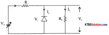
The Zener diode starts conducting only when the source voltage Vs is greater than the Zener breakdown voltage Vz.
When Vs is increased from 0V, load current IL increase with applied voltage. Current through Zener diode wit! be zero.
If Vs is more than Vz, the Zener diode breaks down and conducts. Increasing the input voltage further increases the voltage across the resistor Rs and voltage across load VL remains constant at Vz.
Line regulation :
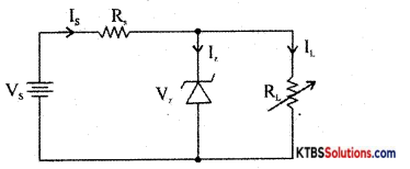
For load regulation, Vs is made greater than Vz. Vs is kept constant and load resistance RL. is varied. If RL is decreased, current IL increases and IL decreases by the same value, but output voltage VL = Vz remains constant.
If RL is increased, IL decreases and Iz increases, but output voltage VL = Vz remains constant.