Students can Download 1st PUC Electronics Previous Year Question Paper March 2015 (North), Karnataka 1st PUC Electronics Model Question Papers with Answers helps you to revise the complete syllabus.
Karnataka 1st PUC Electronics Previous Year Question Paper March 2015 (North)
Time: 3.15 Hours
Max Marks: 70
Instructions:
- The question paper has five Parts A, B, C, D, and E.
- Part – A is compulsory,
- Part – D has only problems.
- Read the instructions given for each part.
PART-A
Answer all Ten questions: (10 × 1 = 10)
Question 1.
Who discovered the Electron?
Answer:
J.J. Thomson.
Question 2.
What is the direction of Conventional Current flow?
Answer:
The direction of conventional current is opposite to that of the flow of electrons.
Question 3.
Expand ECG
Answer:
Electro Cardiogram.
Question 4.
State Ohm’s law.
Answer:
The current flowing through a conductor is directly proportional to the potential difference across the ends of the conductor when the temperature and other physical conditions of the conductor are kept constant.
Question 5.
Define the phase difference between two A.C. quantities.
Answer:
The phase difference between two A.C. quantities is the angular separation between two similar points of the two A.C. quantities.
![]()
Question 6.
In which type of biasing is the pn junction Diode resistance is high?
Answer:
Reverse bias.
Question 7.
Draw the schematic symbol of LED.
Answer:

Question 8.
Why is Transistor called a transfer resistor device?
Answer:
The transistor is called a transfer resistor device because it transfers signals from low resistance region to high resistance region.
Question 9.
How many basic symbols are used in the hexadecimal number system?
Answer:
16
Question 10.
Name the type of capacitor having polarity.
Answer:
Electrolytic capacitor.
PART-B
Answer any Five questions. (5 × 2 = 10)
Question 11.
Name two semiconductor materials used in device fabrication.
Answer:
- Germanium
- Silicon.
![]()
Question 12.
Mention any two properties of charges.
Answer:
- Like charges repel and unlike charges attract.
- Charges always reside on the outer surface of a conductor only.
Question 13.
State Rirchhoff s laws.
Answer:
- Kirchhoff’s current law: The algebraic sum of the currents at a node in an electrical circuit is zero.
- Kirchhoffs voltage law: The algebraic sum of EMFs in any closed loop Of a network is equal to the algebraic sum of IR drops in that loop.
Question 14.
Identify the resistor values with the four-color bands.
(i) Orange – Orange – Brown – Silver
(ii) Red – Red – Red – Gold
Answer:
(i) (10 × 3 + 3) × 10 Ω±10% = 330 Ω±10%
(ii) (10 × 2 + 2) × 100 ± 5% = 2200Ω±5%
Question 15.
A 2.5mH inductor is placed in a circuit, where the frequency is 100 kHz and Voltage is 50V. Calculate reactance and peak current.
Answer:
XL = 2πfL = 2(3.14) × 100 × 103 × 2.5 × 10-3
= 1570 Ω
Irms = \(\frac{V}{X_{\mathrm{L}}}=\frac{50}{1570}\) = 0.0318A
Ip = \(\sqrt{2}\) Irms = 1.414 × 0.0318
= 0.0449 A
= 44.9m A.
![]()
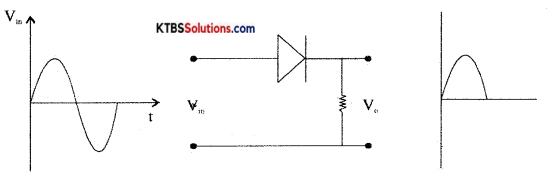
Question 16.
Write the circuit of series negative clippers and show the input and output waveforms.
Answer:
Question 17.
Write the two applications of IR Transistor.
Answer:
- IR transistor is used to pick up IR signal.
- It is used in remote controls of TV, DVD players.
Question 18.
Perform the binary addition of the numbers (1011111)2 and (111011)2.
Answer:

PART-C
Answer any Five questions. (5 × 3 = 15)
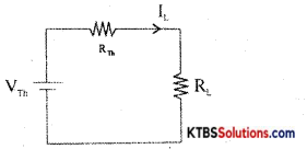
Question 19.
State and explain voltage divider rule.
Answer:
Thevenin’s theorem states that any Linear bilateral network having several voltage sources and resistors can be replaced by a simple circuit having one voltage source V in series with one single resistor Rn.”
Step 1: Identify and remove load resistor RL to convert the circuit as a two-terminal network. Mark the two terminals as A and B.
Step 2: To find VTh, calculate the open-circuit voltage between terminals A and B.
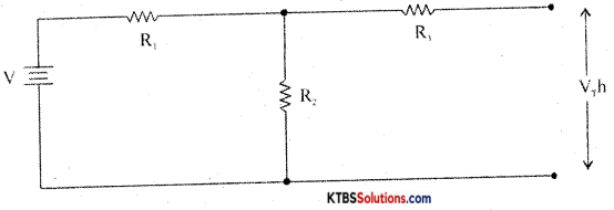
VTh = VR2 = \(\) × R2
Step 3: To find RL, replace all voltage sources in the network with their internal resistances and then find the effective resistance between terminals A and B.
Step 4: Construct Thevenin’s equivalent circuit having VTh in series with RTh and reconnect the load resistor which was earlier removed.
IL = \(\frac{\mathrm{V}_{\mathrm{Th}}}{\mathrm{R}_{\mathrm{Th}}+\mathrm{R}_{\mathrm{L}}}\)
VL = ILRL
Question 20.
Write any three applications of an Oscilloscope.
Answer:
- It is used to measure AC/DC voltage.
- It is used to measure the time period and frequency of ac.
Question 21.
Derive an expression for the effective capacitance of three capacitors connected in series.
Answer:
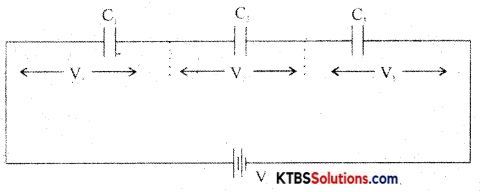
In a series combination, the capacitors are connected end to end. The charge on each capacitor is the same and the emf of the cell equals the sum of voltages across the three resistors.
Consider three capacitors C1, C2, C3 connected in series.
Then V = V1 + V2 + V3
= \(\frac{Q}{C_{1}}+\frac{Q_{1}}{C_{2}}+\frac{Q}{C_{3}}\)
V = Q\(\left(\frac{1}{\mathrm{C}_{1}}+\frac{1}{\mathrm{C}_{2}}+\frac{1}{\mathrm{C}_{3}}\right)\) ……….(1)
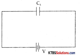
Let the combination be replaced by an equivalent capacitor Cs which has the same effect as the combinations of capacitors. If Cs is the effective capacitance.
then V = \(\frac{\mathrm{Q}}{\mathrm{C}_{\mathrm{s}}}\) → (2)
From equn (1) and (2)
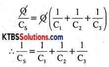
The reciprocal of the effective capacitance of capacitors in series is the sum of reciprocals of individual capacitances.
![]()
Question 22.
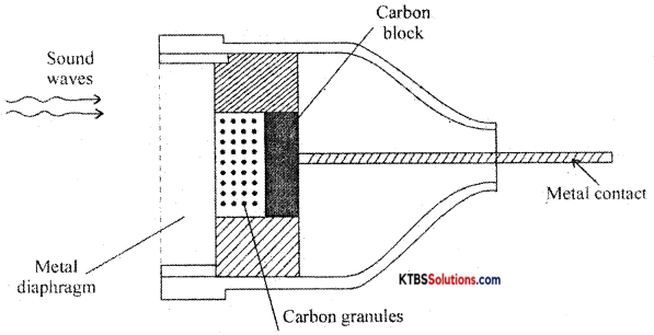
Explain the construction and working of carbon microphones with a diagram.
Answer:
The microphone is a device that converts sound energy into electrical signals. It has an insulating button loosely filled with carbon granules. The button is attached to a very thin steel diaphragm.
The diaphragm vibrates when sound waves strike it. Due to vibration, there is variation in the pressure on carbon granules, which changes the resistance of carbon granules in accordance with the pressure of sound waves.
Hence any change in the resistance of carbon granules produces a corresponding change in the current through the circuit. This varying current flowing through the primary coil produces alternating voltage ¡n the secondary of the transformer.
Question 23.
What is Low Pass Filter? Draw its circuit diagram and frequency response.
Answer:
The low pass filter passes all the low frequencies below a cutoff frequency and stops or attenuates the higher frequencies.
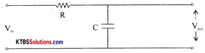
The input is applied across the RC circuit and the output is taken across the capacitor.
At low frequencies, the capacitive reactance X = \(\frac{1}{2 \pi \mathrm{fc}}\) is high and hence entire input voltage appears across the output. At high frequencies, the capacitor offers very low reactance and acts as a short circuit and hence output becomes Zero. The cut off frequency fc = \(\frac{1}{2 \pi \mathrm{fc}}\)
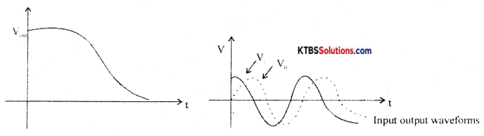
Since the output voltage lags the input voltage, low pass filter ¡s also called lag networks.
Question 24.
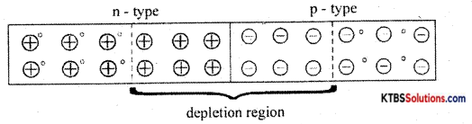
How is the depletion region formed in a p-n junction?
Answer:
A PN junction is formed when one side of a pure semiconductor crystal is doped with a trivalent impurity and the other side with a pentavalent impurity.
The n-type material has electrons as majority charge carriers and holes as minority charge carriers. The p-type material has holes as majority charge carriers and electrons as minority charge carriers. Due to this, there is a concentration gradient across the junction and electrons move from n-type to p-type whereas holes move from p-type to n-type region.
The transfer of electrons and holes across the junction is known as diffusion. The recombination of electrons and holes makes the region near pn junction depleted of electrons and holes.
The depletion region is the region near pn junction which is depleted of mobile charge carriers namely electrons and holes.
The small potential difference developed across the pnj unction due to immobile positive and negative ions is called barrier potential. The barrier voltage is 0.3V for Germanium and 0.7V for silicon. The barrier potential stops the diffusion of charge carriers across the pn junction.
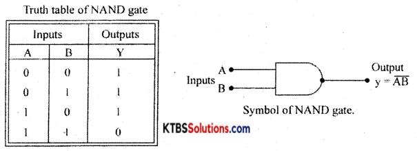
Question 25.
Draw the circuit diagram and explain the working of the DTL NAND Gate.
Answer:
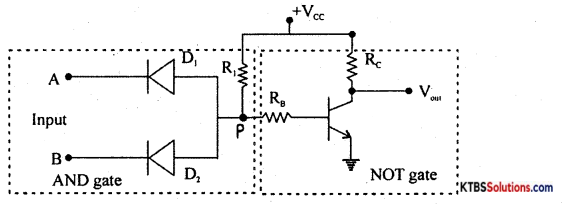
Case (I) When both inputs A and B are LOW (0V), both the diodes D1 and D2 are forward biased. Hence voltage at junction P of the diode becomes zero. This makes the transistor Q go to cut off. Hence the output at the collector of the transistor becomes HIGH.
Case (ii) When A is LOW and B is HIGH, D1 is forward biased and D2 is reverse biased. Hence the voltage at P becomes zero. This makes the transistor go to a cut-off state and therefore output at its collector becomes HIGH.
Case (iii) When A is HIGH and B is LOW, D1 is reverse biased and D2 is forward biased due to which voltage at Pis zero. This makes the transistor go to cut off state and therefore output at its collector becomes HIGH,
Case (iv) When both the inputs are HIGH, D1 and D2 are reverse biased. Hence voltage at P becomes +VOE. This makes the transistor Q go to saturation and the transistor acts like a closed switch. Therefore output becomes LOW.
![]()
Question 26.
Write any three advantages of the Data Sheet.
Answer:
- Product number and name
- Pin connection diagram.
- Absolute minimum, maximum ratings.
- Recommended operating conditions.
- Input/output waveshape diagrams.
PART-D
Answer any three questions: (3 × 5 = 15)
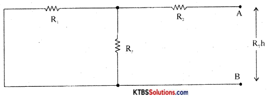
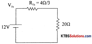
Question 27.
Using Thevenin’s theorem, find the current through 20Ω resistance of the following circuit.
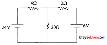
Answer:
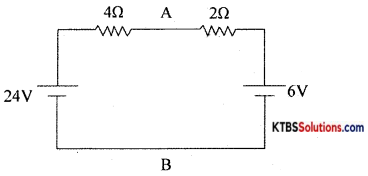
RTh = \(\frac{2 \times 4}{2+4}=\frac{8}{6}=\frac{4}{3}\)
I = \(\frac{24-6}{4+2}=\frac{18}{6}\) = 3A
VAB = 24 – IR = 24 – 3 × 4 = 12V
I = \(\frac{\mathrm{V}_{\mathrm{Th}}}{\mathrm{R}_{\mathrm{Th}}+\mathrm{R}_{\mathrm{L}}}=\frac{12}{20+\frac{4}{3}}=\frac{12 \times 3}{60+4}\) = 0.56A
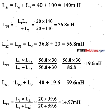
Question 28.
Calculate the equivalent inductance of the following circuit.
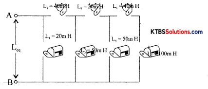
Answer:
Question 29.
(a) An Inductor of 20mH is connected in series with a resistor of 50W The combination is connected to a 220V- 50 Hz source. Find the current in the circuit.
(b) Determine the time constant of an RC circuit when R = 20KΩ and C = 0.05μF.
Answer:
(a) XL =2nfL = 2(3.14)(50)(20 × 10-3)
= 6280Ω
I = \(\frac{V}{X_{L}}=\frac{220}{6280}\) = 0.035A
(b) T = RC = 2 × 103 × 0,05 μF
= 20 × 103 × 0.05 × 10-6
= 10 × 10-3s
= 1ms.
![]()
Question 30.
A 230 V – 50 Hz AC Voltage is applied to the Primary of 5: 1 step down transformer, which is used in Bridge Rectifier, having a load resistance of 100Q. Assuming the Diodes to be ideal, determine the following:
(i) Idc (ii) Vdc (iii) Pdc (iv) PIV
Answer:
V = \(\frac{230}{5}\) = 46V
(i) Idc = \(\sqrt{2}\)Vrms = 0.41A
(ii) Vdc = \(\frac{2 \mathrm{~V}_{\mathrm{m}}}{\pi}=\frac{2 \times 65.05}{3.14}\) = 41.4V
(iii) P = IdcRL = (0.41)2 × 100 = 16.8W
(iv) PIV = 2Vm = 2 × 65.05 = 130.1V
Question 31.
Simply the logic expression.
Y = AB + AC + ABC and draw the logic diaram for the simplified expression using basic gates.
Answer:
Y = AB + AC + AB̅C̅ .
= AB + AB̅C̅ + AC
= A(B + B̅C̅) + AC
= A(B + C̅) + AC
= AB + AC̅ + AC
= AB + A(C̅ + C)
= AB + A.1 (C + C̅ = 1)
= AB + A
= A(B + 1)
= A(1) [B + 1 = 1]
= A.
PART-E
Answer any Four questions. (4 × 5 = 20)
Question 32.
(a) Distinguish between AC and DC. (3 + 2)
(b) Define the following terms:
(i) Cycle (ii) RMS Value
Answer:
- The frequency of AC is the number of AC cycles completed in one second.
- The time period of AC is the time taken to complete one cycle.
- The peak value of AC is the maximum voltage or current of the ac in its one of half cycles.
- RMS value of ac is the equivalent steady DC value which gives the same heating effect as the same rate in a given resistor.
- The peak to the peak value of AC is the maximum value attained in both positive and negative half cycles of AC.
Question 33.
(a) Explain the construction of wire wound resistors.
Answer:
Wire wound resistor is made by winding a wire of known length on a hollow porcelain tube. Eureka wire, an alloy of 60% nickel and 40% copper, is used as a resistance wire. Tinned copper leads are attached to the ends of the winding for connection. The entire assembly is covered with a protective insulation coating of porcelain. The length, thickness, and specific resistivity of the resistance wire determine the resistance value. Their resistance varies from 1 Ω to 1000Ω. They are available with power ratings from 5W to 100W. Wire wound resistors have good stability, reliability, and high power ratings. The resistance value and the power ratings are printed on the body of the resistance. These resistors are used in audio frequency applications.
(b) Write any two applications of LDR.
Answer:
LDRs are used
- to switch on street lights automatically.
- in automatic headlights
- in counters
- in security systems
- in light and dark activated switches and alarms.
Question 34.
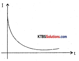
Discuss growth and decay of current in the RL circuit. (3 + 2)
Answer:
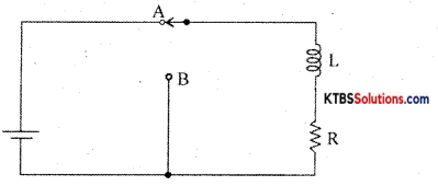
Consider an inductor Land a resistor R connected in series to a cell. When the switch is in position A, the current in the circuit grows exponentially.
The current I at a time after the switch is placed in position A is I = I0e-(R/L)t, where l0 is the maximum current.
The time constant of RL circuits is the time taken by the current to grow to 63.2% of the maximum value.
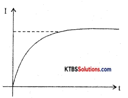
Growth of current in RL circuit
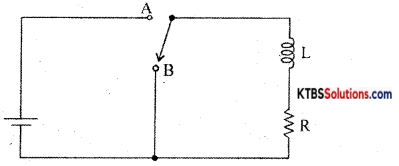
When the switch is in position A, the current in the circuit increases exponentially and reaches a maximum value. When the switch is in position B, the current in the circuit starts decaying exponentially with time.
Decay of current
The value of current at a time after the switch is placed in position B is I = I0e-(R/L)t where l0 is the maximum current.
The time constant of the RL circuit is the time taken by the RL circuit for the current to decay to 36.8% of its maximum value.
![]()
Question 35.
(a) Explain the working of a series Inductor Filter with a circuit diagram. (3 + 2)
Answer:
Filters:
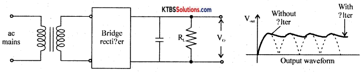
A filter is a circuit that removes AC component from the rectifier output and allows pure DC to reach the load.
Series inductor fitter:
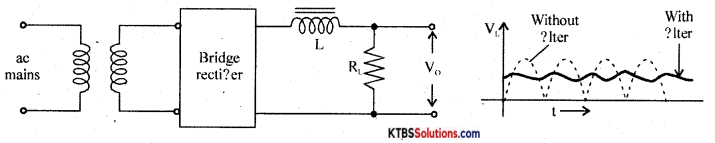
It has an inductor L in series with rectifiers output and loads RL.
The inductor opposes any change in current flowing through it. When the current through the inductor tries to change, a back emf is induced in the inductor which prevents the current from changing. Hence inductor offers a large opposition to the AC component and blocks AC and allows only DC to pass through. Thus DC voltage is developed across RL
Shunt capacitor filter:
It has a large value capacitor connected in parallel with load R.
The capacitor blocks DC and allows AC to pass through. Hence it bypasses the AC component allowing DC to reach the load. Thus shunt capacitor filter removes most of the AC components.
When the output voltage of the rectifier is increasing, the capacitor charges to the peak value of the input. Beyond peak value, the rectifier diode becomes reverse biased and stops conducting.
Now capacitor discharges through RL. The capacitor discharge until the output of the rectifier again increases to a value greater than capacitor voltage. Now diode becomes forward biased and conducts.
Thus the almost constant output is obtained across RL.
LC filter or L type filter:
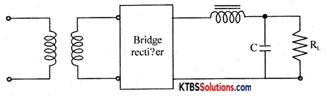
This filter combines the current smoothing action of a series inductor with the voltage stabilizing action of the shunt capacitor filter. The inductor allows DC current to pass through easily offering high reactance to AC.
Any variations or ripple that remains after passing through the inductor are bypassed to the ground by the capacitor. Hence DC voltage reaches the load.
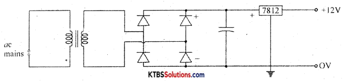
(b) Draw the circuit diagram of the + 12V Voltage Regulator.
Answer:
Question 36.
Explain the working of Zener Diode as a Voltage Regulator with a circuit diagram.
Answer:
In a DC power supply, the output voltage should remain almost constant even as the input and load vary.
Voltages regulation is a measure of the ability of a DC source to maintain a constant output voltage, even whén there is variation in the load resistance or input voltage.
Zener diode as a voltage regulator
Zener diode can be used as a voltage regulator to provide a constant output voltage from a source whose voltage may vary.
The two types of voltage regulators are
- Line regulation
- Load regulation.
Load regulation :
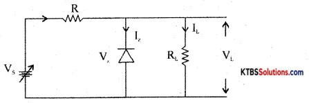
The Zener diode starts conducting only when the source voltage V is greater than Zener breakdown voltage V.
When V is increased from 0V, load current VL increases with applied voltage. The current through Zener diode will be zero.
If V is more than V, the Zener dioðe breaks down and conducts. Increasing the input voltage further increases voltage across the resistor R and voltage across load VL remains constant at V.
Line regulation :
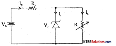
For load regulation, V is made greater than Vz. V is kept constant and load resistance RL is varied. If RL is decreased, current IL increases and Iz decreases by the same value, but output voltage VL = Vz remains constant.
If RL. is increased, I decrease and Iz increases, but output voltage VL = Vz remains constant.
Question 37.
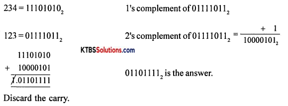
Subtract (123)10 from (234)10 using 2’s complement method.
Answer: