Students can Download 1st PUC Electronics Previous Year Question Paper March 2015 (South), Karnataka 1st PUC Electronics Model Question Papers with Answers helps you to revise the complete syllabus.
Karnataka 1st PUC Electronics Previous Year Question Paper March 2015 (South)
Time: 3.15 Hours
Max Marks: 70
Instructions:
- The question paper has five Parts A, B, C, D and E.
- Part – A is compulsory,
- Part – D has only problems.
- Read the instructions given for each part.
PART – A
Answer all Ten Questions: (10 × 1 = 10)
Question 1.
Expand MOSFET.
Answer:
Metal oxide semiconductor field-effect Transistor.
Question 2.
Mention one limitation of Ohm’s law.
Answer:
Ohms law is not applicable at very low and very high temperatures.
Question 3.
What is the relation between RMS value and peak value of voltage?
Answer:
Vrms = \(\frac{\mathrm{V}_{\mathrm{p}}}{\sqrt{2}}\) or \(\frac{\mathrm{V}_{\mathrm{m}}}{\sqrt{2}}\)
Question 4.
What is the commercial unit of electrical energy?
Answer:
Kilowatt-hour.
![]()
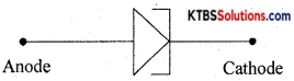
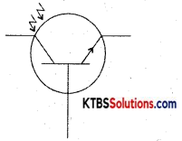
Question 5.
Draw the circuit symbol of the Tunnel diode.
Answer:
Question 6.
What is an ideal diode?
Answer:
An ideal diode is a diode that conducts with zero resistance when forward biased and offers infinite resistance when reverse biased.
Question 7.
Mention the heavily doped region of a transistor.
Answer:
Emitter.
Question 8.
In which mode of operation the transistor is often used as an amplifier?
Answer:
Common emitter mode.
![]()
Question 9.
Convert 1001p) into decimal number system.
Answer:
1 × 23 + 0 × 22 × 21 + 1 × 2° = 8 + 0 + 0 + 1 = 910.
Question 10.
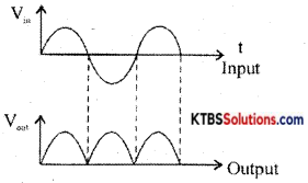
The timing diagram of a logic gate is shown below. Identify the gate
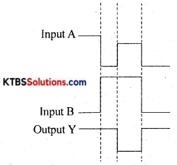
Answer:
NAND Gate.
PART-B
Answer any Five questions. (5 × 2 = 10)
Question 11.
Name the two semiconductor materials used in device fabrication.
Answer:
- Germanium
- Silicon.
Question 12.
Mention any two medical electronic instruments.
Answer:
- Sphygmomanometer
- Glucometer.
Question 13.
Write any two applications of an Oscilloscope.
Answer:
- An oscilloscope is used to measure AC/DC voltages.
- It is used to measure time periods and frequency.
![]()
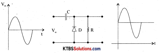
Question 14.
Write the circuit diagram of the positive clamper. Draw the input and output waveforms.
Answer:
Question 15.
Draw the circuit symbol of the IR receiver (transistor). Mention any one application of phototransistor.
Answer:
IR transistors are used in remote controls of TV and DVD players.
Question 16.
A transistor amplifier connected in CE mode has β = 80 and Ic = 5mA. Calculate IE.
Answer:
β = \(\frac{\mathrm{I}_{\mathrm{C}}}{\mathrm{I}_{\mathrm{B}}}\)
80 = \(\frac{5 \times 10^{-3}}{\mathrm{I}_{\mathrm{B}}}\), IB = \(\frac{5 \times 10^{3}}{80}\) = 0.0625 × 10⁻³ A
IE = IB + Ic = 0.0625 × 10⁻³ + 5 × 10-3
= 10-3 (0.0625 + 5)
= 5.0625 × 10⁻³A
= 5.0625 mA.
Question 17.
Draw the circuit diagram of an astable multivibrator using IC 555. Write the expression for frequency.
Answer:
Frequency, f = \(\frac{1.44}{\left(\mathrm{R}_{\mathrm{A}}+2 \mathrm{R}_{\mathrm{B}}\right) \mathrm{C}}\)
Question 18.
Convert AD5(16) into binary and Decimal number systems.
Answer:
AD5(16) =101011010101(2)
AD5(16) = 10 × 162 + 13 × 16′ + 5 × 16°
= 2560 + 208 + 5
= 2773
PART-C
Answer any Five questions. (5 × 3 = 15)
Question 19.
Explain how a DC voltage source is converted into its equivalent current source.
Answer:
The voltage source is that which supplies electrical energy to the circuit in the form of voltage.
RMS value of ac is the equivalent steady DC value that gives the same heating effect at the same rate in a given resistor.
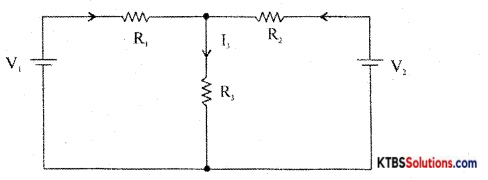
Question 20.
Calculate the current flowing through the 3Ω resistor in the circuit shown below. (use Kirchhoff s laws)
Answer:
4I2 + 2I3 =8
4I2 + 2 × 1 = 8
I2 = \(\frac{6}{4}=\frac{3}{2}\) = 1.5A
I1 = I2 + I3 = 1.5 + 1 = 2.5A
Question 21.
Name the factors on which the inductance of a coil depends. Write the expression for effective inductance, when the inductors are connected in series.
Answer:
Self-inductance of cold depends on
- number of turns in the coil
- length of the coil
- relative permeability of the coil
- The cross-sectional area of the coil.
![]()
Question 22.
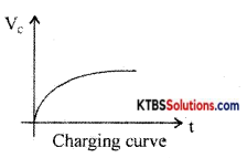
Draw the circuit diagram of the growth of voltage in the RC circuit. Draw the graph of the growth of voltage and write the expression for the instantaneous value of voltage across the capacitor.
Answer:
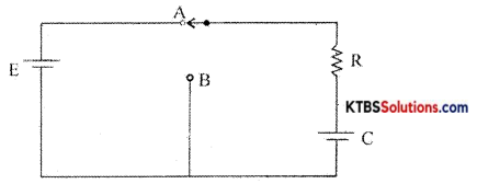
Consider a resistor R and a capacitor C connected in series with a battery of emf E. When the switch is in position A, the capacitor C gets charged through R exponentially with time.
Hence Voltage across the capacitor increases éxponentially and the current in the circuit decreases exponentially. When the capacitor is fully charged, the current becomes Zero. The instantaneous value of voltage across the capacitor during charging is given by
ve = v0(1 – e1/RC)
The instantaneous value of current is I =I0e1/RC Time constant (τ) of an RC circuit is the time taken by the capacitor to charge to 63.2% of maximum current.
Question 23.
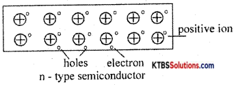
With a lattice structure, explain the n-type semiconductor.
Answer:
n-type semiconductors are semiconductors that are doped with pentavalent impurities like phosphorous, antimony, and arsenic. Each pentavalent atom donates one electron and hence is called donor impurity.
When a pentavalent atom is added, the four valence electrons form covalent bonds with neighboring four silicon atoms and its fifth electron becomes a free electron. The free-electron produced by the pentavalent atom does not create a hole.
When few covalent bonds break due to thermal energy, electrons and holes are created. Thus there will be a large number of free electrons. Hence in n-type material, there are electrons as majority charge carriers and holes as minority charge carriers. The pentavalent impurity atom becomes an immobile positive ion after donating an electron.
The n-type material is electrically neutral because a number of free electrons equal the sum of positive holes and positive ions.
Question 24.
Draw the circuit diagram of the bridge rectifier. Draw the input and output waveforms. Mention is the application of a rectifier.
Answer:
The bridge rectifier does not require a center tap transformer. It uses four diodes D1, D2, D3, and D4 connected in the form of a bridge across the secondary of the transformer.
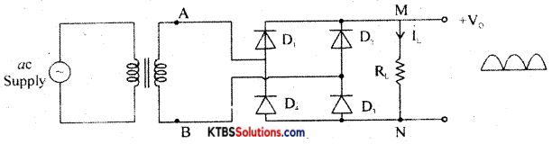
During the positive half cycle of AC input, A is at positive potential and B is not at negative potential. D diodes D1 and D3 are forward biased and conduct. The current flows through AD1MND1B. D2 and D4 do not conduct as they are reverse biased. Thus the positive half cycle of voltage ¡s obtained across the load resistor RL.
During the negative half cycle of AC input, A is at negative potential and B is at positive potential.
Diodes D2 and D4 are forward biased and conduct. Diodes D1 and D1 are reverse biased and do not conduct. Hence current flows along BD2MND4A. Thus a positive half cycle of voltage is developed across the load resistor RL. In both the half cycles, current flows through RL in the same direction from M to N.
Thus varying DC output is obtained across RL.
RMS value of voltage is Vrms = \(\frac{\mathrm{V}_{\mathrm{m}}}{\sqrt{2}}\)
Ripple factor is the ratio of the RMS value of the AC component of the load voltage to the average value of load voltage.
r = Ripple factor = \(\frac{\mathrm{V}_{\text {rims }}}{\mathrm{V}_{\mathrm{avg}}}=\sqrt{\left(\frac{\mathrm{I}_{\mathrm{ms} \mathrm{s}}}{\mathrm{I}_{\mathrm{d}}}\right)^{2}}\) – 1 = 0.48
Efficiency (η) is the ratio of output DC power to the input AC power.
η = \(\frac{\text { DC output power }}{\text { AC input power }}\) r = 0.812 or 81.2%
Question 25.
With a diagram, explain the working of LCD.
Answer:
LCD is a liquid crystal display, is a device that operates by applying a varying electric voltage to the layer of liquid crystal. It does not radiate its own light but reflects light.
LCDs are used in laptop computers. LCD monitors and LCD TVs, calculators, and electronic watches.
![]()
Question 26.
Mention any two types of fixed resistors. Name the chemical used for the etching process in PCB designing.
Answer:
- Wire wound resistor.
- Carbon film resistor,
Ferric chloride.
PART-D
Answer any three questions: (3 × 5 = 15)
Question 27.
(a) Calculate the maximum power delivered to the load RL in the circuit given below.
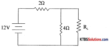
Answer:
VTh = \(\frac{12 \times 4}{2+4}=\frac{48}{6}\) = 8Ω
RTh = \(\frac{2 \times 4}{2+4}=\frac{8}{6}\) = 1.33Ω = RL
PL(max) = \(\frac{V_{t h}^{2}}{4 R_{L}}=\frac{8^{2}}{4 \times 1.33}\) = 12.03W
(b) Find the resistance between A and B in the circuit shown below.

Answer:
\(\frac{1}{\mathrm{R}_{\mathrm{P}}}=\frac{1}{3}+\frac{1}{6}+\frac{1}{12}=\frac{4+2+1}{12}=\frac{7}{12}\)
Rp = \(\frac{12}{7}\)Ω = 1.71Ω
Question 28.
Two capacitors of capacitances 20pF and 80pF are connected in series across 200V DC supply.
Find (i) the equivalent capacitance,
(ii) the charges on each capacitor and
(iii) potential difference across each capacitor.
Answer:
Ceff = \(\frac{C_{1} C_{2}}{C_{1}+C_{2}}=\frac{20 \times 80}{20+80}\) = 16μF
Q = Ceff V = 16 × 10-6 × 200 = 3.2mC
V1 = \(\frac{\mathrm{Q}}{\mathrm{C}_{1}}=\frac{3.2 \times 10^{-3}}{20 \times 10^{-6}}\) = 160V
V2 = \(\frac{\mathrm{Q}}{\mathrm{C}_{2}}=\frac{3.2 \times 10^{-3}}{80 \times 10^{-6}}\) = 40V
Question 29.
(a) Determine the time constant of RL circuit is 5ms. If L = 10mH, calculate the value of resistance.
(b) A series RLC circuit has R = 20Ω, C = 100nF, L = 100mH. Calculate resonant frequency.
Answer:
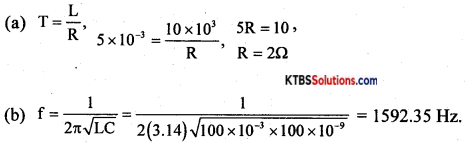
Question 30.
Determine the minimum value of RL that will turn the Zener diode on in the Zener regulator circuit. Given Vs = 18V = 1KΩ and V, = 8V. If the load resistance RL is 2kΩ, calculate Zener current.
Answer:
RL(min) = \(\frac{\mathrm{R}_{\mathrm{S}} \mathrm{V}_{\mathrm{Z}}}{\mathrm{V}_{\mathrm{S}}-\mathrm{V}_{\mathrm{Z}}}=\frac{1000 \times 8}{18-8}\) = 800Ω
Is = \(\frac{18-8}{1000}\) = 10mA
IL = \(\frac{V_{z}}{R_{L}}=\frac{8}{2000}\) =4mA
Iz = Is – IL = 10 – 4 = 6mA.
Question 31.
(a) Simplify the following Boolean expression and draw the logic diagram for the simplified expression. y= \(\overline{\overline{\mathbf{A B}+\mathbf{A C}}+\overline{\mathbf{A B C}}}\)
Answer:
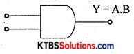
Y = \(\overline{\overline{\mathbf{A B}+\mathbf{A C}}+\overline{\mathbf{A B C}}}\)
= \(\overline{\overline{\mathrm{AB}+\mathrm{AC}}}+\overline{\overline{\mathrm{AB}} \mathrm{C}}\)
= (AB + AC).\(\overline{\overline{\mathrm{AB}} \cdot \mathrm{C}}\)
= (AB + AC).(\(\overline{\overline{\mathrm{AB}}}\) + C̅)
= (AB + AC)(AB + C̅)
= AB.AB + ABC̅ + ACAB+ACC̅
= AB + ABC̅ + ABC + O (Q CC̅ = 0)
= AB(1 + C̅ + C)
= AB . 1
= AB.
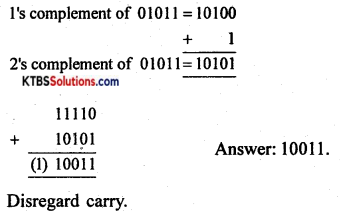
(b) Subtract 1011(2) from 11110(2) using 2’s complement method.
Answer:
PART-E
Answer any four questions. (4 × 5 = 20)
Question 32.
State and explain the superposition theorem with an example.
Answer:
In any linear bilateral network consisting of two or more independent sources, the resultant current or voltage in any branch is the algebraic sum of the currents or voltages caused by each independent source acting alone, with all other independent sources being replaced by their internal resistances.
Procedure for using Superposition Theorem:
Step 1: Retain the source V1 and replace all other sources with their internal resistances.
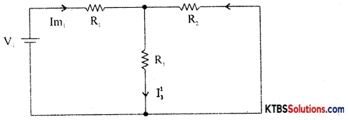
Step 2: Current in various branches and their voltage drops due to V1 alone are determined as follows,
RT1 = R1 + \(\frac{\mathrm{R}_{2} \mathrm{R}_{3}}{\mathrm{R}_{2}+\mathrm{R}_{3}}\)
Im1 = \(\frac{\mathrm{V}_{1}}{\mathrm{R}_{\mathrm{T}_{1}}}\)
I’3 = Im1 × \(\frac{R_{2}}{R_{2}+R_{3}}\) {from branch current formula}
Voltage across R3 = V’3 = I’3 = I”1 = Im2 × \(\frac{R_{1}}{R_{1}+R_{3}}\)
Step 3 : Consider V2 alone and find the currents and voltages as follows:
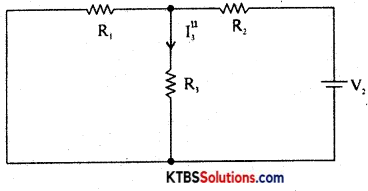
RT2 = R2 + \(\frac{\mathrm{R}_{1} \mathrm{R}_{3}}{\mathrm{R}_{1}+\mathrm{R}_{3}}\)
Im2 = \(\frac{\mathrm{V}_{2}}{\mathrm{R}_{\mathrm{T}_{2}}}\)
I”3 = V2 × \(\frac{\mathrm{R}_{1}}{\mathrm{R}_{1}+\mathrm{R}_{3}}\)
Step 4: Find the algebraic sum of currents and voltage drops in a branch.
I3 = I’3 + I”3; V’3 = I’3R3, V = I”3R3
V3 = V’3 + V”3
Question 33.
With a diagram, explain the construction and working of the relay. Mention any two applications of the transformer.
Answer:
Chokes are used in
- tube light sets
- in radio ànd TV receivers
- in power supplies
- in RF tuning circuits.
Relays arc used
- as protective device
- to realize logic functions
- as counters
- as an automatic switching device to operate Street lights, UPS, buzzers.
![]()
Question 34.
With a diagram, explain the construction and working of a loudspeaker. Mention one application of the microphone.
Answer:
A loudspeaker is a transducer that changes eleçtrical energy into sound waves of varying pressure.
- a coil of wire called a voice coil.
- a permanent magnet
- a cone-shaped piece of stiff paper or cloth called the diaphragm.
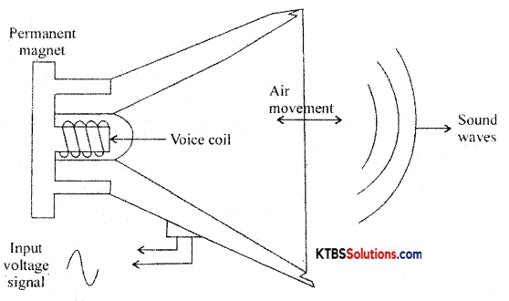
Voice coil is suspended in the strong magnetic field of a circular permanent magnet. The permanent magnet of a speaker provides a steady magnetic field. The two leads of the voice coil are connected with wire to terminals on the speaker frame.
When the audio signal current flows through the voice coil, it produces varying magnetic fields in the coil. The varying magnetic field moves the voice coil in and out in accordance with variations in the electrical audio signals. Hence the diaphragm attached to the voice coil vibrates due to which compressions and rarefactions are formed and the sound waves are produced.
Question 35.
(a) Draw the circuit diagram of the low pass filter. Draw the frequency response curve. Write the expression for cut-off frequency.
Answer:
The low pass filter passes all the low frequencies below a cutoff frequency and stops or anticipates the higher frequencies.
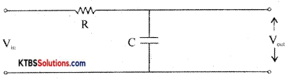
The input is applied across the RC circuit and the output is taken across the capacitor. At low frequencies, the capacitive reactance X = \(\frac{1}{2 \pi \mathrm{fc}}\) is high and hence entire input voltage appears across the output. At high frequencies, the capacitor offers very low reactance and acts as a short circuit and hence output becomes Zero. The cut off frequency fc = \(\frac{1}{2 \pi \mathrm{fc}}\)
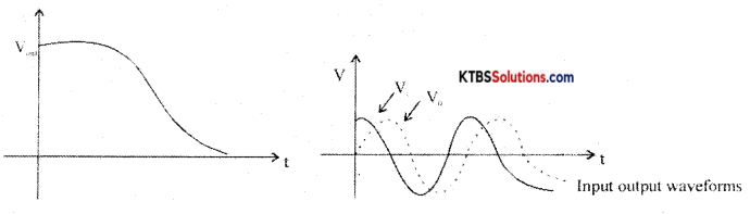
Since the output voltage lags the input voltage, a low pass filter is also called a lag network.
(b) Define quality factor and power factor.
Answer:
The quality factor of a circuit is the ratio of resonant frequency to the bandwidth.
![]()
Question 36.
With a circuit diagram, explain an experiment to draw the forward and reverse bias characteristics of a semiconductor diode. Draw the curves.
Answer:
The V-I characteristic of a diode is the graph between the voltage across the diode and the current flowing through it.
The V-I characteristics can be divided into two parts namely
- Forward characteristics
- Reverse characteristics.
1. Forward characteristics of semiconductor diode:
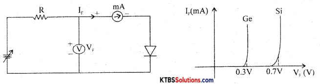
The circuit for plotting V-I characteristics of the diode is as shown. The resistance R limits the current to a permissible value. A voltmeter measures the voltage across the diode and the milliammeter reads the current flowing through the diode.
The forward voltage VF is increased in steps of 0.1 V and the corresponding forward current IF, is noted. A graph of VF along the x-axis and corresponding IF, along the y-axis gives the forward characteristics curve.
Diode current VF is zero when VF 0. When VF is more than barrier potential, current IF increases. The forward voltage VF at which forward current starts to increase rapidly is called the knee voltage or cut-in voltage or threshold voltage (VK). For germanium diode, = 0.3 V and for silicon diode, VK = 0.7V.
Reverse characteristics of a pn junction:
The circuit for plotting reverse characteristics of a diode is shown below
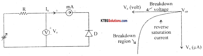
The reverse voltage is increased gradually till the diode starts conducting and the corresponding reverse currents are noted. On platting a graph between reverse voltage and reverse current, the characteristic curve is as showñ.
Due to reverse bias applied on pn junction, an extremely small current ‘R (few iA) flows through the diode. The reverse current remains almost constant up to the breakdown voltage. After this point, for a small change in reverse voltage, the reverse current increases very rapidly. This sudden flow of large current may destroy the diode due to overheating. Hence, the diode should be operated in the reverse bias with reverse voltage less than break down voltage.
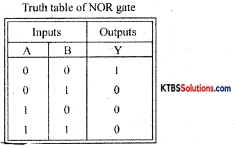
Question 37.
Draw the circuit diagram of two input DTL NOR gates. Explain it’s working. Write its truth table and logic symbol.
Answer:
NOR gate is a logic circuit whose output is HIGH only when both its inputs are LOW
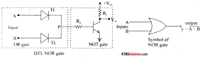
Diodes D1 and D2 form OR gates and the transistor act as NOT gate.
Case (1) When A = 0, B = 0, the diodes are not forward biased and they do not conduct. Hence voltage P is zero. This zero voltage makes the transistor go to cut-off condition and therefore output is HIGH.
Case (ii) When A= 0, B = 1, D1 does not conduct but D2 conducts. Hence voltage at P is +Vcc and it drives the transistor to saturation and output becomes LOW.
Case (iii) When A = 1, B = 0, D1 conducts and D2 does not conduct. Hence voltage at P is +Vcc and this makes the transistor Q go to saturation. Hence output becomes LOW.
Case (iv) When A = I, B = 1, both diodes conduct as they are forward biased. Then voltage at P is +Vcc and the transistor is driven to saturation. The output at the collector becomes LOW.