Students can Download 1st PUC Electronics Previous Year Question Paper March 2016 (North), Karnataka 1st PUC Electronics Model Question Papers with Answers helps you to revise the complete syllabus.
Karnataka 1st PUC Electronics Previous Year Question Paper March 2016 (North)
Time: 3.15 Hours
Max Marks: 70
Instructions:
- The question paper has five Parts A, B, C, D, and E.
- Part – A is compulsory,
- Part – D has only problems.
- Read the instructions given for each part.
PART-A
Answer ALL questions: (10 × 1 = 10)
Question 1.
Expand www.
Answer:
World Wide Web.
Question 2.
Write the S.I unit of charge.
Answer:
Coulomb.
Question 3.
What is a node?
Answer:
Node is a point in a circuit where more than three resistors meet.
Question 4.
What is inductance?
Answer:
Inductance is the property of an element or circuit which when carrying a current is characterized by the formation of a magnetic field and storage of magnetic energy.
Question 5.
What is a high pass filter?
Answer:
A high pass filter passes all the frequencies above the cut-off frequency f and rejects all the frequencies below f.
![]()
Question 6.
Name anyone trivalent impurity material.
Answer:
Gallium
Question 7.
Write the names of scientists who invented the transistor.
Answer:
William Shockley, John Bardeen, and Walter Brattain.
Question 8.
Mention the application of common collector configuration.
Answer:
As buffer amplifier.
Question 9.
What is Nibble?
Answer:
A nibble is a group of four bits.
Question 10.
Write the logic symbol of NOT gate.
Answer:

PART-B
Answer any Five questions. (5 x 2 = 10)
Question 11.
Mention a few applications of electronics.
Answer:
(a) Entertainment
(b) Communication.
Question 12.
Write the advantages of a multimeter.
Answer:
(a) It is inexpensive
(b) Measurements are accurate.
Question 13.
What is a transducer? Write the name of one transducer.
Answer:
- The transducer is a device that converts one form of energy into another.
- Loudspeaker.
![]()
Question 14.
Calculate the inductive reactance of a 3 mH inductor connected to an AC of 230V, 50Hz.
Answer:
XL = 2πfL = 2 × 3.14 × 50 × 3 × 10-3
= 942 × 10-3
= 0.942 Ω.
Question 15.
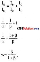
Derive the relationship between a and p of a transistor.
Answer:
IE = IB + Ic
Divide throughout by Ic
Question 16.
Write the circuit diagram of CE transistor characteristics. Mention any one transistor configuration.
Answer:
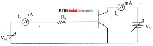
- Common Base transistor configuration.
Question 17.
Convert the binary number (1111)2 to decimal number.
Answer:
(1111)2
= 1 × 23 + 1 × 22+ 1 × 2′ + 1 × 2°
= 8+ 4 + 2 + 1 = 15
Question 18.
Simplfy the Boolean equation Y = AB + A\((\overline{B+C})\).
Answer:
Y = AB + A\((\overline{B+C})\)
= AB + A(B̅C̅)
= AB + AB̅C̅
= A(B + B̅C̅)
= A(B + C̅)
= AB + AC̅.
PART-C
Answer any Five questions. (5 × 3 = 15)
Question 19.
Write the limitations of Ohm’s law.
Answer:
- Ohm’s law is not valid at very low and very high temperatures.
- When the physical conditions of a conductor change, Ohms law is not valid.
- Ohm’s law is not applicable to semiconductors, discharge tubes, and electrolytes.
Question 20.
Calculate the effective capacitance between A and B for the circuit given below.
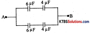
Answer:
Cs1 = \(\frac{\mathrm{C}_{1} \mathrm{C}_{2}}{\mathrm{C}_{1}+\mathrm{C}_{2}}=\frac{6 \times 4}{6+4}\) = 2.4 μF
Cs2 = \(\frac{\mathrm{C}_{3} \mathrm{C}_{4}}{\mathrm{C}_{3}+\mathrm{C}_{4}}=\frac{6 \times 4}{6+4}\) 2.4 μF
Cpp = Cs1 + CS2 = 2.4 + 2.4 = 4.8 pF.
![]()
Question 21.
A neat diagram explains the construction of the carbon film resistor.
Answer:
Wire wound resistor is made by winding a wire of known length on a hollow porcelin tube. Eureka wire, an alloy of 60% nickel and 40% copper, is used as a resistance wire. Tinned copper leads are attached to the ends of the winding for connection. The entire assembly is covered with a protective insulation coating of porcelain. The length, thickness, and specific resistivity of the resistance wire determine the resistance value. Their resistance varies from 1Ω to 1000Ω. They are available with a power ratings from 5W to 100W. Wire wound resistors have good stability, reliability, and high power ratings. The resistance value and the power ratings are printed on the body of the resistance. These resistors are used ¡n audio frequency applications.
Question 22.
Write the properties of semiconductors.
Answer:
- Semiconductors are tetravalent and hence covalent bonding takes place between their atoms.
- At absolute zero, semiconductors behave like a perfect insulator.
- Resistance of semiconductors decreases when their temperature is increased (α the temperature coefficient of resistance is negative)
- The conductivity of semiconductors can be increased by adding suitable impurities to them.
Question 23.
Write a diagram explain the formation of N-type semiconductors.
Answer:
n-type semiconductors are semiconductors that are doped with pentavalent impurities like phosphorous, antimony, and arsenic. Each pentavalent atom donates one electron and hence is called donor impurity. ,
When a pentavalent atom is added, the four valence electrons form covalent bonds with neighboring four silicon atoms and its fifth electron becomes a free electron. The free-electron produced by the pentavalent atom does not create a hole.
When few covalent bonds break due to thermal energy, electrons and holes are created. Thus there will be a large number of free electrons. Hence in n-type material, there are electrons as majority charge carriers and holes as minority charge carriers. The pentavalent impurity atom becomes an immobile positive ion after donating an electron.
Question 24.
Explain the working of the series negative clippers, with a diagram.
Answer:
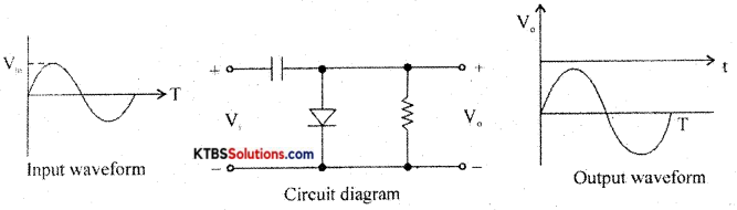
A negative clamper is a circuit that clamps the negative peak of a signal to a desired de level.
Question 25.
Write the diagram and explain the working of the shunt capacitor fitter.
Answer:
Filters:
A filter is a circuit which removes AC component from the rectifier output and allows pure
DC to reach the load.
Series inductor filter:
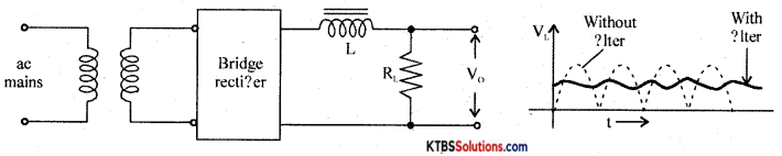
It has an inductor L in series with rectifiers output and loads RL.
The inductor opposes any change in current flowing through it. When the current through the inductor tries to change, a back emf is induced in the inductor which prevents the current from changing. Hence inductor offers a large opposition to the AC component and blocks AC and allows only DC to pass through. Thus DC voltage is developed across RL
Shunt capacitor filter:
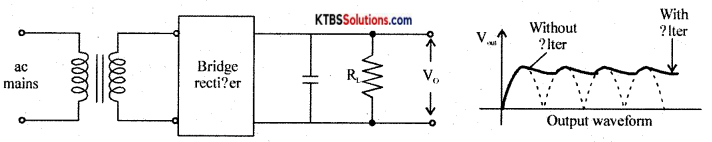
It has a large value capacitor connected in parallel with load RL.
The capacitor blocks DC and allows AC to pass through. Hence it bypasses the AC component allowing DC to reach the load. Thus shunt capacitor filter removes most of the AC components.
When the output voltage of the rectifier is increasing, the capacitor charges to the peak value of the input. Beyond peak value, the rectifier diode becomes reverse biased and stops conducting.
Now capacitor discharges through RL. The capacitor discharge until the output of the rectifier again increases to a value greater than capacitor voltage. Now diode becomes forward biased and conducts.
Thus almost constant oütput is obtained across R1.
LC filter or L type filter:
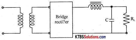
This filter combines the current smoothing action of a series inductor with the voltage stabilizing action of the shunt capacitor filter. The inductor allows DC current to pass through easily offering high reactance to AC.
Any variations or ripple that remains after passing through the inductor are bypassed to the ground by the capacitor. Hence DC voltage reaches the load.
![]()
Question 26.
Briefly explain PCB drilling and PCB assembling.
Answer:
PCB layout preparation: PCB layout must be drawn using PC. The complete circuit must be drawn on paper. Prepare computer layout as per circuit diagram using PCB design software.
Draw tracks for connecting one component to the other. Take printout on a white sheet and get the film done on a transparent sheet by filmmakers.
Photoresist: Photoresist film or mask is placed on a copper clad board. UV light is exposed on a copper-clad board covered by photoresist film. UV light does not pass through the photoresist on the tracks. The copper area which is not covered protected by photo-resist is removed during the etching process.
PCB etching process: The etching process is done to remove the unnecessary copper after UV exposure, leaving behind only the desired copper tracks. The PCB is then dipped in fern chloride or hydrochloric acid until unwanted copper is dissolved.
Then the PCB is dipped in acetone to remove the black color giving the PCB a shining attractive look. ,
PCB Drilling: The components to be attached to PCB can be done only by vias drilling i.e, by drilling a hole. To make PCB good solderable the surface of the PCB is coated with tin or nickel.
PCB assembling: The electronic components are assembled on the respective holes in the PCB. The component leads are electrically and mechanically fixed to the board with solder.
PART-D
Answer any three questions: (3 × 5 = 15)
Question 27.
Find Vm, Vp-p, Vrms, Vavg, and frequency of the given ac waveform.
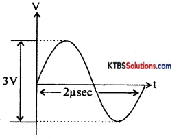
Answer:
Vm = \(\frac{3}{2}\) = 1.5V
Vp-p = 3V
Vrms = \(\frac{\mathrm{V}_{\mathrm{m}}}{\sqrt{2}}=\frac{1.5}{\sqrt{2}}\) = 1.06V
Vavg = \(\frac{2 \mathrm{~V}_{\mathrm{m}}}{\pi}=\frac{2 \times 1.5}{3.14}\) = 0.95 V
Question 28.
(a) Two capacitors plates separated by air, each of effective area 4 × 10⁴m2 is separated by 1.4 × 10⁻³. Find its capacitance.
(b) Find the energy stored in a 1 μH inductor, when a current of 10 mA is flowing through it.
Answer:
A = 4 × 10⁻⁴ m2, d = 1.4 × 10⁻³m
(a) C = \(\frac{\varepsilon_{0} A}{d}=\frac{8.854 \times 10^{-12} \times 4 \times 10^{-4}}{1.4 \times 10^{-3}}\)
= \(\frac{8.854 \times 4}{1.4}\) × 10-13
= 25.29 × 10⁻¹³ F.
(b) E = \(\frac{1}{2}\) LI2
= \(\frac{1}{2}\) × 1 × 10-6 × (10 × 10-3)2
= \(\frac{1}{2}\) × 10-6 × 100 × 10-6
= 50 × 10-12 J.
Question 29.
A 20Ω resistance in series with inductance XL = 60. and capacitance Xc = 30Ω. The applied voltage is V = 60mV with 50Hz. Calculate impedance, current, and phase angle.
Answer:
R = 20Ω
Z = \(\sqrt{\mathrm{R}^{2}+\left(\mathrm{X}_{\mathrm{L}}-\mathrm{X}_{\mathrm{c}}\right)^{2}}\)
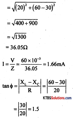
Φ = tan-1(1.5) = 56°19′
Question 30.
A center-tapped transformer has a 230V primary winding and a secondary winding rated at 15V-0-15V and is used in a full-wave rectifier circuit with a load of 120Ω. Calculate dc output voltage, dc load current, and the PIV rating required for diode?
Answer:
Vp = 230V, RL = 120
Peak supply voltage, Vm = Vms × \(\sqrt{2}\)
= 15 × \(\sqrt{2}\)
= 21.21V.
Load resistance = 120Ω
DC output voltage, Vdc = \(\frac{2 V_{\mathrm{m}}}{\pi}\) = 13.5V
DC load current, Idc = \(\frac{2 I_{m}}{\pi}=\frac{2 V_{m}}{\pi R_{L}}\)
= \(\frac{2 \times 21.21}{\pi \times 120}\) = 0.11 A
PIV rating of diodes = 2Vm = 2 × 15\(\sqrt{2}\)
= 42.43V.
![]()
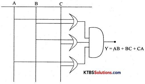
Question 31.
Draw the logic diagram for the Boolean equation Y = AB + BC + CA.
Answer:
PART – E
Answer any Four questions. (4 × 5 = 20)
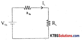
Question 32.
State and explain Thevenin’s theorem.
Answer:
Thevenin’s theorem states that any linear bilateral network having several voltage sources and resistors can be replaced by a simple circuit having one voltage source V in series with one single resistor RTh.”
Step 1: Identify and remove load resistor RL to convert the circuit as a two-terminal network. Mark the two terminals as A and B.
Step 2: To find V, calculate the open-circuit voltage between terminals A and B.
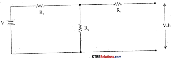
VTh = VR2 = \(\frac{V}{R_{1}+R_{2}}\) × R2
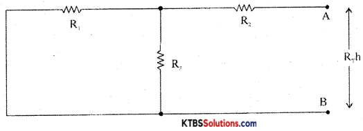
Step 4: Construct Thevenin’s equivalent circuit having V in series with R and reconnect the load resistor which was earlier removed.
IL = \(\frac{\mathrm{V}_{\mathrm{Th}}}{\mathrm{R}_{\mathrm{Th}}+\mathrm{R}_{\mathrm{L}}}\)
VL = ILRL
Question 33.
Explain the construction and working of the thermistor.
Answer:
Thermistors are used in
- temperature measurement
- temperature control in air conditioners.
- alarm systems
- liquid level detection.
Question 34.
Derive an expression for the equivalent capacitance of two capacitors connected in series.
Answer:
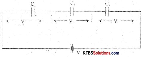
In a series combination, the capacitors are connected end to end. The charge on each capacitor is the same and the emf of the cell equals the sum of voltages across the three resistors.
Consider three capacitors C1, C2, C3 connected in series.
ThenV = V1 + V2 + V3.
= \(\frac{Q}{C_{1}}+\frac{Q_{1}}{C_{2}}+\frac{Q}{C_{3}}\)
V = Q\(\left(\frac{1}{\mathrm{C}_{1}}+\frac{1}{\mathrm{C}_{2}}+\frac{1}{\mathrm{C}_{3}}\right)\)………(1)
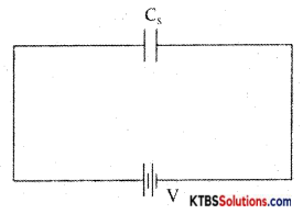
Let the combination be replaced by an equivalent capacitor Cs which has the same effect as the combinations of capacitors. If C is the effective capacitance.
then V = \(\frac{\mathrm{Q}}{\mathrm{C}_{\mathrm{S}}}\) → (2)
From equn (1) and (2)
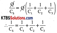
The reciprocal of the effective capacitance of capacitors in series is the sum of reciprocals of individual capacitances.
Question 35.
(a) Explain the growth of current in the RL circuit. (3 + 2)
Answer:
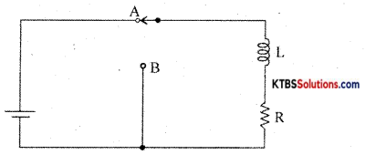
Consider an inductor Land a resistor R connected in series to a cell. When the switch is in position A, the current in the circuit grows exponentially.
The current I at a time after the switch is placed in position A is I = I0e-(R/L)t, where I0 is the maximum current.
The time constant of RL circuits is the time taken by the current to grow to 63.2% of the maximum value.
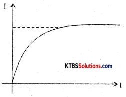
(b) Write the equation of the time constant and also define the time constant.
Answer:
t = \(\frac{\mathrm{L}}{\mathrm{R}}\)
The time constant is the time taken by the capacitor to charge to 63.2% of the supply voltage.
![]()
Question 36.
(a) What is a varactor diode?
Answer:
Varactor diode which acts as a variable capacitor under reverse biased condition.
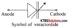
They are used in LC tuned circuits, TV receivers, FM receivers.
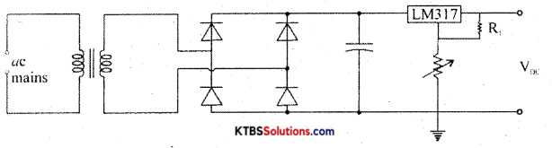
(b) Explain the working of the fixed positive regulated power supply using IC 7812 and write the circuit diagram. (1 + 4)
Answer:
Question 37.
(a) Explain the working of the DTL NAND gate. (3 + 2)
Answer:
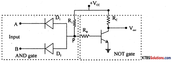
Case (I) When both inputs A and B are LOW (0V), both the diodes D1 and D2 are forward biased. Hence voltage at junction P of the diode becomes zero. This makes the transistor Q go to cut off. Hence the output at the collector of the transistor becomes HIGH.
Case (ii) When A is LOW and B is HIGH, D1 is forward biased and D2 ¡s reverse biased. Hence the voltage at P becomes zero. This makes the transistor go to a cut-off state and therefore output at its collector becomes HIGH.
Case (iii) When A is HIGH and B is LOW, D1 ¡s reverse biased and D2 is forward biased due to which voltage at Pis zero. This makes the transistor go to a cut-off state and therefore output at its collector becomes HIGH.
Case (iv) When both the inputs are HIGH, D1 and D2 are reverse biased. Hence voltage at P becomes +VOE. This makes the transistor Q to go to saturation and transistor acts like a closed switch . Therefore output becomes LOW.
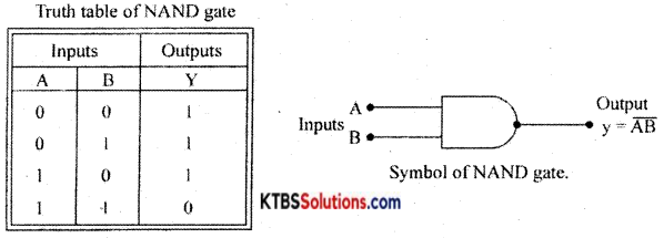
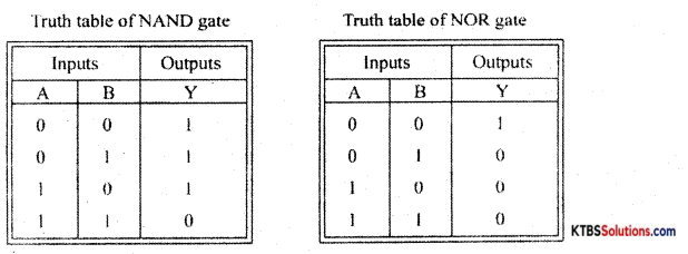
(b) Write the symbol and truth table of NAND gate.
Answer: