Students can Download 1st PUC Electronics Previous Year Question Paper March 2016 (South), Karnataka 1st PUC Electronics Model Question Papers with Answers helps you to revise the complete syllabus.
Karnataka 1st PUC Electronics Previous Year Question Paper March 2016 (South)
Time: 3.15 Hours
Max Marks: 70
Instructions:
- The question paper has five Parts A, B, C, D, and E.
- Part – A is compulsory,
- Part – D has only problems.
- Read the instructions given for each part.
PART-A
Answer all Ten questions: (10 × 1 = 10)
Question 1.
What is the SI unit of electric power?
Answer:
Watt.
Question 2.
Is Ohm’s law applicable to semiconductors?
Answer:
No.
Question 3.
What is meant by thermistor?
Answer:
It is a temperature-sensitive semiconductor device.
Question 4.
What is a low pass filter?
Answer:
A filter circuit that allows all the low-frequency signals from 0 Hz to cut off frequency.
![]()
Question 5.
What is a clamper circuit?
Answer:
A circuit that keeps either the positive peak or negative peak of a signal at the desired dc level.
Question 6.
Draw the symbol of the Schottky diode.
Answer:
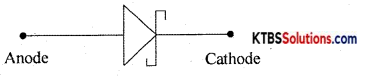
Question 7.
Which region of the transistor is largest in size?
Answer:
Collector.
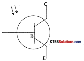
Question 8.
Draw the symbol of the phototransistor.
Answer:
Question 9.
Define NAND gate.
Answer:
NAND gate is a logic gate whose output is low only when all its inputs are HIGH.
Question 10.
Write 1’s complement of (1011)2.
Answer:
0100.
PART-B
Answer any Five questions. (5 × 2 = 10)
Question 11.
What are a pulse oximeter and ultrasound scan?
Answer:
- Pulse oximeter: It is a medical instrument used to detect the saturation level of hemoglobin content of humans.
- Ultra scan: It is a test that uses sound waves to create images of organs and structures inside the body.
Question 12.
Mention any two applications of an oscilloscope.
Answer:
- It is used to measure AC/DC voltage.
- It is used to measure the time period and frequency of ac.
![]()
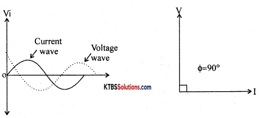
Question 13.
Show the graphical and phasor diagram representation of the phase relation between the voltage and current in an ac circuit containing only a pure inductor.
Answer:
Question 14.
What is an intrinsic and extrinsic semiconductor?
Answer:
- Intrinsic semiconductor: A semiconductor in its extremely pure form is known as an intrinsic semiconductor.
- Extrinsic semiconductor: A doped semiconductor is known as an extrinsic semiconductor.
Question 15.
Mention the majority and minority charge carriers in the n-p-n transistor.
Answer:
- Majority carriers – Electrons
- Minority carriers – Holes.
Question 16.
The current gain of a transistor in CE mode is 200. Calculate the collector current when the base current is 20μA.
Answer:
Ic = βIB
Ic = 200 × 20 × 10-6 = 4 × 10³A = 4mA
Question 17.
Simplify the Boolean expression Y = A.B + A.\((\overline{B+C})\).
Answer:
Y = A.B + A.\((\overline{B+C})\)
= AB + A.(B̅.C̅)
= A.B + AB̅C̅
= A(B + B̅C̅)
= A(B + C̅)
= AB + AC̅
Question 18.
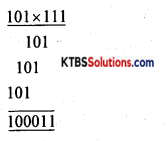
Multiply (101)2 with (111)2.
Answer:
PART-C
Answer any Five questions. (5 × 3 = 15)
Question 19.
(a) Mention any two communication applications of electronics.
Answer:
- Internet
- telephone
(b) Expand SCR.
Answer:
Silicon Controlled Rectifier.
![]()
Question 20.
Mention any three properties of electrical charges.
Answer:
- Like charges repel and unlike charges attract each other.
- Charges can neither be created nor be destroyed.
- Charges take only integral values.
- Charges on a body are not affected by the motion of the body.
- Charges always reside only on the outer surface of a conductor only.
Question 21.
An ac voltage in volts is given by V = 310 sin 314t. Find the frequency, average voltage and rms voltage.
Answer:
(i) Frequency,
Compare with V = Vm sin ωt,
f = \(\frac{w}{2 \pi}=\frac{314}{6.284}\)
= 49.96 ≈ 50Hz.
(ii) V = 0.637 × Vm =0.637 × 310V
= 197.47V
(iii) Vms = \(\frac{\mathrm{V}_{\mathrm{m}}}{\sqrt{2}}\) = 0.707 × 310V
= 219.17V.
Question 22.
Derive an expression for effective resistance of two resistors connected in parallel.
Answer:
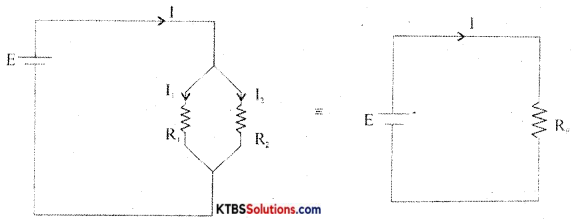
Consider two resistors R1 and R2 connected in parallel between the same two common points.
In parallel combination, the voltage across each resistor is the same.
Let I1 and I2 be the currents through the resistors R1 and R2.
The current from the cell equals the sum of the currents through the two resistors, i.e.,
I = I1 + I2 = \(\frac{V}{R_{1}}+\frac{V}{R_{2}}\) = V\(\left(\frac{1}{R_{1}}+\frac{1}{R_{2}}\right)\) → (1)
Equivalent or effective resistor Rp is a single resistor that has the same effect as a tile parallel combination. If Rp is the effective resistor, then I = \(\frac{\mathrm{V}}{\mathrm{Rp}}\) → (2)
From equation (1) and (2)
\(\frac{\mathrm{V}}{\mathrm{Rp}}\) = V\(\left(\frac{1}{R_{1}}+\frac{1}{R_{2}}\right)\)
\(\frac{1}{\mathrm{Rp}}=\frac{1}{\mathrm{R}_{1}}+\frac{1}{\mathrm{R}_{2}}\)
Hence, the reciprocal of effective resistance of a number of resistors in parallel is the sum of the reciprocals of the individual resistances.
![]()
Question 23.
With a circuit diagram, briefly explain the working of the series inductor filter.
Answer:
Filters:
A filter is a circuit that removes the AC component from the rectifier output and allows pure DC to reach the load.
Series inductor filter:
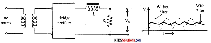
It has an inductor L in series with rectifiers output and loads RL.
The inductor opposes any change in current flowing through it. When the current through the inductor tries to change, a back emf is induced in the inductor which prevents the current from changing. Hence inductor offers a large opposition to the AC component and blocks AC and allows only DC to pass through. Thus DC voltage is developed across RL.
Shunt capacitor filter:
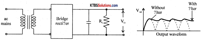
It has a large value capacitor connected in parallel with load R.
The capacitor blocks DC and allows AC to pass through. Hence it bypasses the AC component allowing DC to reach the load. Thus shunt capacitor filter removes most of the AC components.
When the output voltage of the rectifier is increasing, the capacitor charges to the peak value of the input. Beyond peak value, the rectifier diode becomes reverse biased and stops conducting.
Now capacitor discharges through RL. The capacitor discharge until the output of the rectifier again increases to a value greater than capacitor voltage. Now diode becomes forward biased and conducts.
Thus the almost constant output is obtained across RL.
LC filter or L type filter:
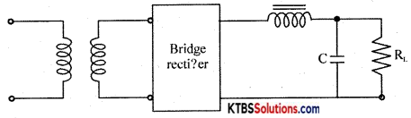
This filter combines the current smoothing action of a series inductor with the voltage stabilizing action of the shunt capacitor filter. The inductor allows DC current to pass through easily offering high reactance to AC.
Any variations or ripple that remains after passing through the inductor is bypassed to the ground by the capacitor. Hence DC voltage reaches the load.
Question 24.
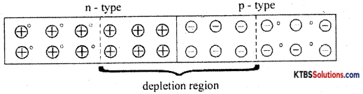
With a diagram, briefly explain the formation of the depletion region in the unbiased semiconductor diode.
Answer:
A PN junction is formed when one side of a pure semiconductor crystal is doped with a trivalent impurity and the other side with a pentavalent impurity.
The n-type material has electrons as majority charge carriers and holes as minority charge carriers. The p-type material has holes as majority charge carriers and electrons as minority charge carriers. Due to this, there is a concentration gradient across the junction and electrons move from n-type to p-type whereas holes move from p-type to n-type region.
The transfer of electrons and holes across the junction is known as diffusion. The recombination of electrons and holes makes the region near pn junction depleted of electrons and holes.
The depletion region is the region near pn junction which is depleted of mobile charge carriers namely electrons and holes.
The small potential difference developed across the PN junction due to immobile positive and negative ions is called barrier potential. The barrier voltage is 0.3V for Germanium and 0.7V for silicon. The barrier potential stops the diffusion of charge carriers across the PN junction.
Question 25.
Mention any three applications of LED.
Answer:
- In inductor lamps and displays.
- In optical communication system.
- In seven segment display.
![]()
Question 26.
(a) Expand PCB
Answer:
Printed Circuit Board.
(b) Mention any two advantages of PCB.
Answer:
- The circuit will look neat without any wires falling apart.
- Much higher density components are placed with PCB.
PART-D
Answer any three questions: (3 × 5 = 15)
Question 27.
Using Thevenin’s theorem find the current through RL = 10Ω
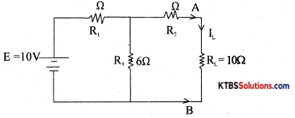
Answer:
R = (3Ω ∥6Ω) + 4Ω
= 6Ω
VTh = E\(\left(\frac{R_{3}}{R_{1}+R_{3}}\right)\) = 10V\(\left(\frac{6 \Omega}{3 \Omega+6 \Omega}\right)\) = 6.66V
IL = \(\frac{\mathrm{V}_{\mathrm{Th}}}{\left(\mathrm{R}_{\mathrm{Th}}+\mathrm{R}_{\mathrm{L}}\right)}=\frac{6.66}{6+10}\) = 0.416A
Question 28.
Calculate the capacitance of the capacitor C3 in the given capacitive circuit, if the equivalent capacitance of the combination between A and B is 15μF.
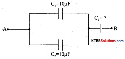
Answer:
(C1 parallel C2) series with C3
Cp = C1 + C2 = 10 + 10 = 20μF
Cs = \(\frac{C_{\mathrm{P}} \times C_{3}}{C_{P}+C_{3}}\)
15 = \(\frac{20 \times C_{3}}{20+C_{3}}\)
15C3 + 300 = 20C3
300 = 20C3– 15C3
300 = 5C3
C3 = 60μF.
![]()
Question 29.
An unknown capacitor, a 5Ω resistor and an inductor of 50mH are in series with an ac source of 100V, 50Hz. It is found that the current is inphase with voltage. Determine
(i) Capacitance of unknown capacitor
Answer:
f = \(\frac{1}{2 \pi \sqrt{\mathrm{LC}}}\) or C = \(\frac{1}{4 \pi^{2} f^{2} L}\)
C = 202.53μF
(ii) Impedance of the circuit
Answer:
z = \(\sqrt{\mathrm{R}^{2}+\left(\mathrm{X}_{\mathrm{L}}-\mathrm{X}_{\mathrm{C}}\right)^{2}}\)
or
Z = R because XL = Xc at resonance
Z = 5Ω
(iii) Current in the circuit.
Answer:
I = \(\frac{V}{Z}=\frac{100 V}{5}\) = 20A
Question 30.
For a zener diode voltage regulator with applied volatage of Vs = 10V, series resistor of Rs = 50Ω, Zener diode with zener voltage Vz = 6V and load resistor RL = 390Ω, Zener diode with zener voltage Vz = 6V and load resistor RL = 390Q. Determine
(i) Load voltage
Answer:
Load voltage Vz = VL = 6V
(ii) Voltage drop across series resistance
Answer:
Voltage across series resistor VRs = Vs – Vz
VRs = 10V – 6V = 4V
(iii) Current through the zener diode and
Answer:
Zener current, Iz = Is – IL
Iz = \(\frac{V_{s}-V_{z}}{R_{s}}-\frac{V_{z}}{R_{L}}\)
= \(\frac{\mathrm{V}_{\mathrm{RS}}}{\mathrm{R}_{\mathrm{s}}}-\frac{\mathrm{V}_{\mathrm{z}}}{\mathrm{R}_{\mathrm{L}}}\)
= \(\frac{4 V}{50 \Omega}-\frac{6 V}{300 \Omega}\)
= 0.065A = 65mA
(iv) RL(min)
Answer:
RL(min) = \(\frac{R_{\mathrm{s}} \cdot V_{\mathrm{z}}}{\mathrm{V}_{\mathrm{s}}-V_{\mathrm{z}}}\)
= \(\frac{50 \times 60}{10-6}=\frac{300}{4}\) = 75Ω
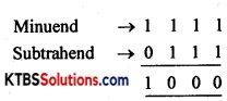
Question 31.
Subtract (111)2 from (1111)2 using 2’s complement method. Also, verify the same by direct subtraction method.
Answer:
2’s complement subtraction:
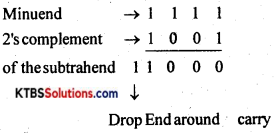
∴ 1000 is the final result.
Direct subtraction:
Answer any four questions. (4 × 5 = 20)
Question 32.
(a) State and explain Ohm’s law.
(b) Determine the resistance value of an electrical appliance marked with 220V, 550W. (3 + 2)
Answer:
(a) The current flowing through a conductor is directly proportional to the potential difference across its ends, provided the temperature and other physical conditions remain constant”.
V = IR
where ‘R’ is the constant of proportionality known as the resistance of a resistor.
(b) R = \(\frac{\mathrm{V}^{2}}{\mathrm{P}}\) = 88Ω
![]()
Question 33.
(a) Briefly explain the construction and working of transformer.
Answer:
Ferrite core inductor: In ferrite core inductors, the wire is wound over a solid ferrite core. Ferrite is a synthetic ceramic material that ¡s highly ferromagnetic. Ferrites are insulators that provide high permeability. These have inductance values up to 10 mH.
![]()
Ferrite Core
Ferrite core inductors are used as filter chokes and in TV receivers.
Iron core inductor: in iron core inductors, the coil is wound on a solid laminated iron core. The core is laminated to avoid eddy current losses. A laminated iròn core is made up of thin iron laminations pressed together but insulated from each other. These have high inductance values from 1 mH to 1H.
![]()
Symbol of iron core inductor
(b) Does a transformer work on DC? (4 + 1)
Answer:
No.
Question 34.
Explain the construction and working of moving coil type loudspeaker.
Answer:
A loudspeaker is a transducer that changes electrical energy into sound waves of varying pressure.
- a coil of wire called a voice coil.
- a permanent magnet
- a cone-shaped piece of stiff paper or cloth called the diaphragm.
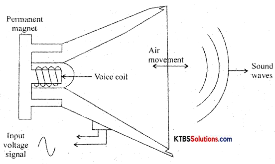
Voice coil is suspended in the strong magnetic field of a circular permanent magnet. The permanent magnet of a speaker provides a steady magnetic field. The two leads of the voice coil are connected with wire to terminals on the speaker frame.
When audio signal current flows through the voice coil, it produces varying magnetic fields in the coil. The varying magnetic field moves the voice coil in and out in accordance with variations in the electrical audio signals. Hence the diaphragm attached to the voice coil vibrates due to which compressions and rarefactions are formed and the sound waves are produced.
Question 35.
(a) With a circuit diagram and graph, Explain the growth of current in an RL circuit.
Answer:
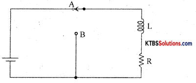
Consider an inductor Land a resistor R connected in series to a cell. When the switch is in position A, the current in the circuit grows exponentially.
The current I at a time after the switch is placed ¡n the position A is I = I0e-(R/L)t, where I0 is the maximum current.
The time constant of RL circuits is the time taken by the current to grow to 63.2% of the maximum value.
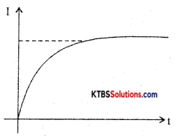
Growth of current in RL circuit
(b) Define quality factors in an ac circuit.
Answer:
The quality factor of a circuit is the ratio of resonant frequency to the bandwidth.
![]()
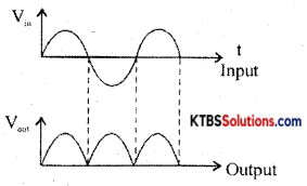
Question 36.
With a circuit diagram showing input and rectified output signal waveforms, briefly explain the working of a full-wave bridge rectifier.
Answer:
The bridge rectifier does not require a center tap transformer. It uses four diodes D1, D2, D3, and D4 connected in the form of a bridge across the secondary of the transformer.
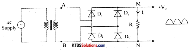
During the positive half cycle of AC input, A is at positive potential and B is not at negative potential. D codes D1, and D3 are forward biased and conduct. The current flows through AD1MND1B. D2 and D4 do not conduct as they are reverse biased. Thus the positive half cycle of voltage ¡s obtained across the load resistor RL.
During the negative half cycle of AC input, A is at negative potential and B is at positive potential.
Diodes D2 and D4 are forward biased and conduct. Diodes D1 and D3 are reverse biased and do not conduct. Hence current flows along BD2MND4A. Thus a positive half cycle of voltage is developed across the load resistor RL. In both the half cycles, current flows through RL in the same direction from M to N.
Thus varying DC output is obtained across RL.
RMS value of voltage is V = \(\frac{\mathrm{V}_{\mathrm{m}}}{\sqrt{2}}\)
Ripple factor is the ratio of the RMS value of the AC component of the load voltage to the average value of load voltage.
r = Ripple factor = \(\frac{V_{\text {rims }}}{V_{\text {avg }}}=\sqrt{\left(\frac{I_{\text {ms }}}{I_{d}}\right)^{2}}\) 1 = 0.48
Efficiency (η) is the ratio of output DC power to the input AC power.
η = \(\frac{\text { DC output power }}{\text { AC input power }}\) r = 0.812 or 81.2%
Question 37.
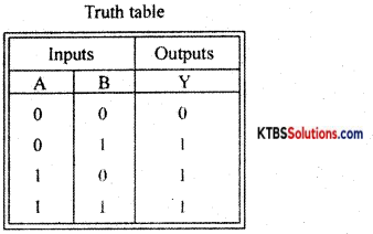
With the help of the circuit diagram and truth table, explain the working of two input diode OR -gate.
Answer:
OR gate is a logic circuit whose output is LOW only when all its inputs are LOW.
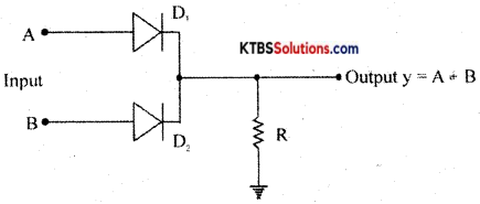
Case (I) When A = 0, B = 0, both the diodes are not conducting. No current flows through resistor R1 and hence output y 0.
Case (ii) When A = 0, B = 1, D1 is reverse biased and does not conduct. D1 is forward biased and conducts. Hence current flows through R. making output y = 1.
Case (iii) When A = 1, B = 0, D1 conducts as it is forward biassed, and D2 does not conduct as it is reverse biased. The current flows through RL and output y I.
Case (iv) When A = I, B = 1, both the diodes conduct as they are forward biased. The current flows through R1 making output y HIGH.