Students can Download 1st PUC Electronics Previous Year Question Paper March 2017 (North), Karnataka 1st PUC Electronics Model Question Papers with Answers helps you to revise the complete syllabus.
Karnataka 1st PUC Electronics Previous Year Question Paper March 2017 (North)
Time: 3.15 Hours
Max Marks: 70
Instructions:
- The question paper contains four parts.
- Part-A has no choice.
- Part – D contains two subparts: (i) Problems (ii) Essay-type questions.
- Draw the circuit diagrams wherever necessary.
PART-A
Answer ALL questions: (10 × 1 = 10)
Question 1.
Expand RAM.
Answer:
Random-access memory.
Question 2.
Write the unit of electric power.
Answer:
Watt.
Question 3.
When will a load receive maximum power from a source?
Answer:
RL = RTh
Question 4.
Define temperature co-efficient of a material.
Answer:
The temperature coefficient of resistance is the ratio of increase in resistance per °C rise in temperature to its resistance at 0°C.
Question 5.
What is meant by the power factor of an A.C. circuit?
Answer:
Power factor is the ratio of active power to apparent power.
![]()
Question 6.
What is the forward resistance value of an ideal P-N junction diode?
Answer:
Zero.
Question 7.
Draw the circuit symbol of the photodiode.
Answer:

Question 8.
Which region of the transistor is made thin and lightly doped?
Answer:
Base
Question 9.
What is a Nibble?
Answer:
Group of four bits.
Question 10.
Convert (36)16 into decimal equivalent.
Answer:
(36)16 = 3 × 161 + 6 × 16° = 48 + 6 = (54)10.
PART-B
Answer any Five questions.
Question 11.
Mention any two communication applications of electronics.
Answer:
(a) Wi-Fi
(b) Cellphones
Question 12.
Write any two applications of ECG
Answer:
To assess the functioning of the heart.
![]()
Question 13.
Sketch the symbols of (i) AC voltmeter and (ii) DC ammeter.
Answer:
(i) AC voltmeter

(ii) DC Ammeter

Question 14.
(a) Define the time constant of an RC circuit during the growth of voltage across a capacitor, (b) Write an expression of average AC power.
Answer:
- The time constant of an RC circuit is defined as the time taken by the capacitor to charge to 63.2% of the supply voltage.
- P = Vrms Irms cosΦ.
Question 15.
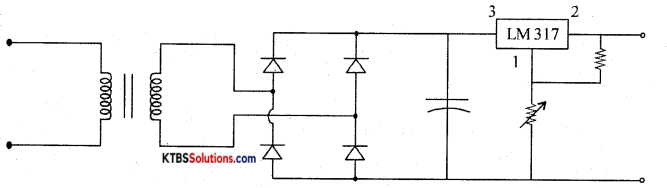
Draw the circuit diagram of the adjustable regulated power supply using LM 317.
Answer:
Question 16.
Following current readings are obtained in a transistor circuit. IE = 2mA and IB= 20μA. Calculate the values of α and Ic.
Answer:
IE = 2mA; IB=20μA = 20 × 103mA = 0.02mA; Ic = IE – IB = 2 – 0.02 = 1.98 mA.
α = \(\frac{\mathrm{I}_{\mathrm{C}}}{\mathrm{I}_{\mathrm{E}}}=\frac{1.98}{2}\) = 0.99
![]()
Question 17.
State De-Morgan’s theorems.
Answer:
- Complement of a logical sum is equal to logical product of complements.
\(\overline{\mathrm{A}+\mathrm{B}}\) = A̅. B̅ - Complement of a logical product is equal to the logical sum of the complements.
\(\overline{\text { A.B }}\) = A̅ + B̅
Question 18.
Prove that (A + B) (B + C) = B + A.C.
Answer:
LHS = (A + B) (B + C)
= AB + AC + B.B + BC
– AB + AC + B + BC (Q BB = B)
= AB + AC + B (1 +C)
= AB + AC + B.l
= AB + AC + B
= B(A + 1) + AC
= B + AC (Q A + 1 = 1)
= RHS.
PART-C
Answer any Five questions. (5 × 3 = 15)
Question 19.
State ohms law. Mention its two limitations.
Answer:
Ohms law states that current through a conductor is proportional to the potential difference across its ends when the temperature and other physical conditions are kept constant.
It can not be applied
- at very low and at very high temperatures,
- to semiconductors.
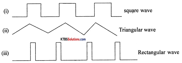
Question 20.
Draw three non-sinusoidal waveforms.
Answer:
Question 21.
With the help of a diagram, explain the construction of the wire-wound resistor.
Answer:
Wire wound resistor is made by winding a wire of known length on a hollow porcelain tube. Eureka wire, an alloy of 60% nickel and 40% copper, is used as a resistance wire. Tinned copper leads are attached to the ends of the winding for connection. The entire assembly is covered with a protective insulation coating of porcelain. The length, thickness, and specific resistivity of the resistance wire determine the resistance value. Their resistance varies from 1 Ω to 1000Ω. They are available with power ratings from 5W to 100W. Wire wound resistors have good stability, reliability, and high power ratings. The resistance value and the power ratings are printed on the body of the resistance. These resistors are used in audio frequency applications.
![]()
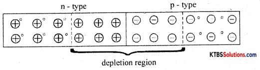
Question 22.
What is the depletion region? What happens to the depletion layer of pn junction when it is forward biased and reverse biased?
Answer:
A PN junction is formed when one side of a pure semiconductor crystal is doped with a trivalent impurity and the other side with a pentavalent impurity.
The n-type material has electrons as majority charge carriers and holes as minority charge carriers. The p-type material has holes as majority charge carriers and electrons as minority charge carriers. Due to this, there is a concentration gradient across the junction and electrons move from n-type to p-type whereas holes move from p-type to n-type region.
The transfer of electrons and holes across the junction is known as diffusion. The recombination of electrons and holes makes the region near pn junction depleted of electrons and holes.
The depletion region is the region near pn junction which is depleted of mobile charge carriers namely electrons and holes.
The small potential difference developed across the pn junction due to immobile positive and negative ions is called barrier potential. The barrier voltage is 0.3V for Germanium and 0.7V for silicon. The barrier potential stops the diffusion of charge carriers across the pn junction.
Question 23.
Draw the circuit diagram of the full-wave, bridge rectifier. Also, showing its input and rectified output waveforms.
Answer:
The bridge rectifier does not require a center tap transformer. It uses four diodes D1, D2, D3, and D4 connected in the form of a bridge across the secondary of the transformer.
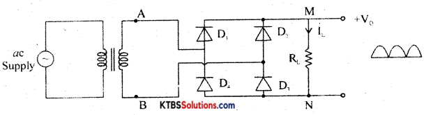
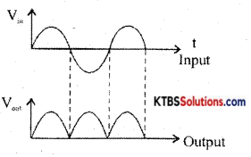
During the positive half cycle of AC input, A is at positive potential and B is not at negative potential. D diodes D1 and D3 are forward biased and conduct. The current flows through AD1MND1B. D2 and D4 do not conduct as they are reverse biased. Thus the positive half cycle of voltage is obtained across the load resistor R.
During the negative half cycle of AC input, A is at negative potential and B is at positive potential.
Diodes D2 and D4 are forward biased and conduct. Diodes D1 and D3 are reverse biased and do not conduct. Hence current flows along BD3MND4A. Thus a positive half cycle of voltage is developed across the load resistor RL. In both the half cycles, current flows through RL in the same direction from M to N.
Thus varying DC output is obtained across RL.
RMS value of voltage is Vrms = \(\frac{\mathrm{V}_{\mathrm{m}}}{\sqrt{2}}\)
Ripple factor is the ratio of the RMS value of the AC component of the load voltage to the average value of load voltage.
r = Ripple factor = \(\frac{V_{\text {rins }}}{V_{\text {avg }}}=\sqrt{\left(\frac{I_{\mathrm{rms}}}{I_{\mathrm{d}}}\right)^{2}}\) – 1 = 0.48
Efficiency (η) is the ratio of output DC power to the input AC power.
η = \(\frac{\text { DC output power }}{\text { AC input power }}\) r = 0.812 or 81.2%
Question 24.
Give any three applications of LED.
Answer:
- LED is used as an indicator lamp.
- In optical fiber communication
- LED is used in the solid-state video display.
![]()
Question 25.
With a circuit diagram explain the working of the NPN transistor.
Answer:
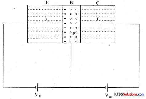
The emitter-base junction is forward biased by power supply VE and the collector-base junction is reverse biased by the power supply V.
The negative terminal of V repels the majority charge carriers electrons in the n-type emitter towards the base region. When VEE is greater than the barrier potential of the emitter-base junction the electrons from the emitter region move to the p-type base region. This forms the emitter current
The base is thin and has only a few electrons. Hence only a few electrons and holes recombine and this forms the base current ‘VE’ The remaining free electrons in the base region move to the collector region attracted by the +Vcc. They move through the collector region into +Vcc, This forms collector current Ic.
The relation connecting the currents ¡n the transistor is IE = IB + Ic
Question 26.
(a) What is meant by 2 × 16 LCD?
Answer:
2 × 16 LCD means 2 lines 16 characters display
(b) Briefly explain the process during PCB designing.
Answer:
PCB layout preparation: PCB layout must be drawn using PC. The complete circuit must be drawn on paper. Prepare computer layout as per circuit diagram using PCB design software.
Draw tracks for connecting one component to the other. Take printout on a white sheet and get the film done on a transparent sheet by filling makers.
Photoresist: Photoresist film or mask is placed on a copper clad board. UV light ¡s exposed on copper clad board covered by photoresist film. UV light does not pass through the photoresist on the tracks. The copper area which is not covered protected by photo-resist is removed during the etching process.
PCB etching process: The etching process is done to remove the unnecessary copper after UV exposure, leaving behind only the desired copper tracks. The PCB is then dipped in fern chloride or hydrochloric acid until unwanted copper is dissolved. Then the PCB is dipped in acetone to remove the black color giving the PCB a shining attractive look.
PCB Drilling: The components to be attached to PCB can be done only by vias drilling Je, by drilling a hole. To make PCB good solderable the surface of the PCB is coated with tin or nickel.
PCB assembling: The electronic components are assembled on the respective holes in the
PCB. The component leads are electrically and mechanically fixed to the board with solder.
PART-D
Answer any three questions: (3 × 5 = 15)
Question 27.
Using Kirchhoff s laws, find the branch currents in the resistive network given :
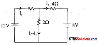
Answer:
Apply KVL to ABEFA,
6I1 + 2(I1 – I2) – 12 = 0
8I1 – 2I2 = 12
4I1 – I2 = 6 ………(1)
Apply KVL to BCDEB,
4I2 + 8 – 2 (I1 – I2) = 0
I1 – 3I2 = 4 ……..(2)
Solving equations (1) and (2)
I1 =1.27 A
I2 = -0.909A
I3 = I1 – I2 = 2.181 A.
![]()
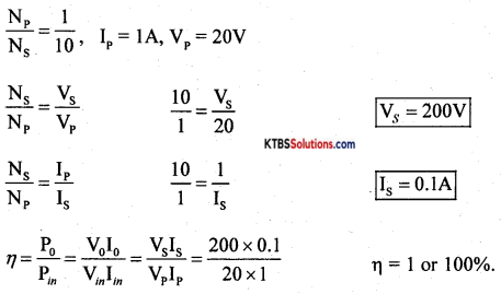
Question 28.
In a transformer, if the primary to secondary turns ratio is 1: 10 and current and voltage in the primary coil is 1A and 20V respectively, calculate:
(i) Current and voltage in the secondary.
(ii)Efficiency of the transformer.
Answer:
Question 29.
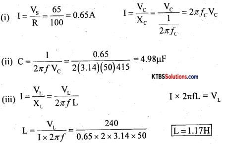
A series LCR circuit is connected to an AC voltage source of 220V, 50Hz. If the voltage across the resistor is 65V, the voltage across the capacitor is 415V, and that across the inductor is 240V, calculate (i) current flowing in the circuit; (ii) value of the capacitor
(iii) value of the inductor.
Answer:
Vs = 220V, f = 50Hz; VR = 65V, Vc = 415V, VL = 240V; R = 100Ω
Question 30.
A Zener diode voltage regulated power supply has Vm = 20 V. Rs = 150W, Vz = 12V and RL = 680Ω. Draw the Zener voltage regulator circuit. Also find output voltage, the current through a series resistor, and current through Zener diode.
Answer:
Vm = 20V, Rs = 150Ω Vz = 12V, RL = 680Ω
Is = \(\frac{\mathrm{V}_{\mathrm{s}}}{\mathrm{R}_{\mathrm{s}}}=\frac{8}{150}\) = 0.053A.
IL = \(\frac{\mathrm{V}_{\mathrm{Z}}}{\mathrm{R}_{\mathrm{L}}}=\frac{12}{680}\) = 0.0176A.
Iz = Is – IL = 0.036A
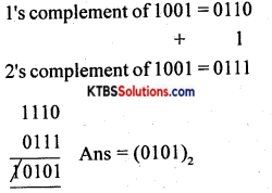
Question 31.
Subtract (9)10 from (14)1(|in binary using 2’s complement subtraction method. Also, verify the same by the direct method.
Answer:
(14)10 = (1110)2, (9)10 = (1001)2
PART – E
Answer any four questions. (4 × 5 = 20)
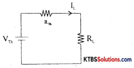
Question 32.
State and explain Thevenin’s theorem.
Answer:
Thevenin’s theorem states that any linear bilateral network having several voltage sources and resistors can be replaced by a simple circuit having one voltage source VTh in series with one single resistor RTh.”
Step 1: Identify and remove load resistor RL to convert the circuit as a two-terminal network. Mark the two terminals as A and B.
Step 2: To find VTh calculate the open-circuit voltage between terminals A and B.
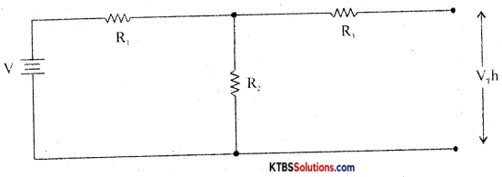
VTh = VR2 = \(\frac{V}{R_{1}+R_{2}}\) × R2
Step 3: To find R, replace all voltage sources in the network with their internal resistances and then find the effective resistance between terminals A and B.
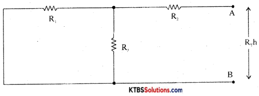
Step 4: Construct Thevenin’s equivalent circuit having VTh in series with RTh and reconnect the load resistor which was earlier removed.
IL = \(\frac{\mathrm{V}_{\mathrm{Th}}}{\mathrm{R}_{\mathrm{Th}}+\mathrm{R}_{\mathrm{L}}}\)
VL = ILRL
![]()
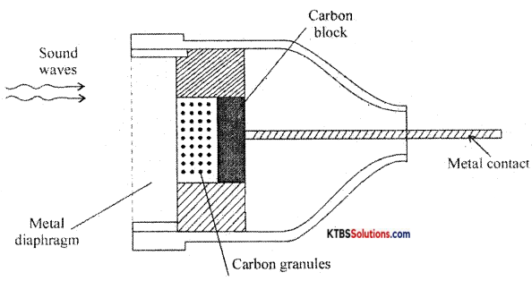
Question 33.
With the help of a labeled diagram write the construction and working of the carbon microphone.
Answer:
The microphone is a device that converts sound energy into an electrical signal. It has an insulating button loosely filled with carbon granules. The button is attached to a very thin steel diaphragm.
The diaphragm vibrates when sound waves strike it. Due to vibration, there is variation in the pressure on carbon granules, which changes the resistance of carbon granules in accordance with the pressure of sound waves.
Hence any change in the resistance of carbon granules produces a corresponding change in the current through the circuit. This varying current flowing through the primary coil produces an alternating voltage in the secondary of the transformer.
Question 34.
(a) Derive an expression for the effective capacitance of three capacitors connected in series.
(b) What is meant by temperature sensors? Write the symbol of LDR.
Answer:
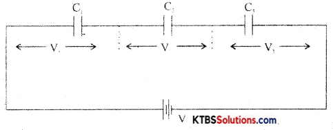
In a series combination, the capacitors are connected end to end. The charge on each capacitor is the same and the emf of the cell equals the sum of voltages across the three resistors.
Consider three capacitors C1, C2, C3 connected in series.
Then V = V1 + V2 + V3
= \(\frac{\mathrm{Q}}{\mathrm{C}_{1}}+\frac{\mathrm{Q}_{1}}{\mathrm{C}_{2}}+\frac{\mathrm{Q}}{\mathrm{C}_{3}}\)
V = Q\(\left(\frac{1}{\mathrm{C}_{1}}+\frac{1}{\mathrm{C}_{2}}+\frac{1}{\mathrm{C}_{3}}\right)\) …………(1)
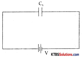
Let the combination be replaced by an equivalent capacitor Cs which has the same effect as the combinations of capacitors. If C is the effective capacitance.
then V = \(\frac{\mathrm{Q}}{\mathrm{C}_{\mathrm{s}}}\) → (2)
From equn (1) and (2)
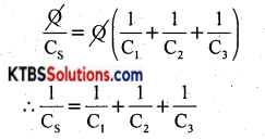
The reciprocal of the effective capacitance of capacitors in series is the sum of reciprocals of individual capacitances.
Question 35.
(a) Derive an expression for the resonance frequency of a series resonance circuit. (3M)
Answer:
Consider an AC circuit consisting of inductance (L), capacitor C and a resistance R connected in series to an AC source. Let the instantaneous voltage of the ac source be
v = Vm sin wt
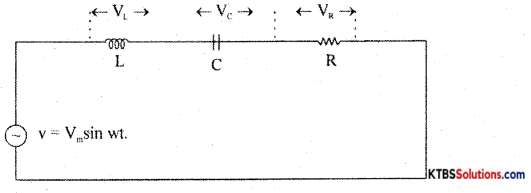
Let VL, VR, Vc be the voltages across the inductor, Resistor, and capacitor.
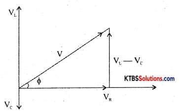
Result voltage V = \(\sqrt{V_{\mathrm{R}^{2}}+\left(\mathrm{V}_{\mathrm{L}}-\mathrm{V}_{\mathrm{C}}\right)^{2}}\)
= \(\sqrt{I^{2} R^{2}+\left(I X_{L}-I X_{C}\right)^{2}}\)
= \(\sqrt{I^{2}\left[R^{2}+\left(X_{L}-X_{C}\right)^{2}\right]}\) = I\(\sqrt{R^{2}+\left(X_{L}-X_{C}\right)^{2}}\)
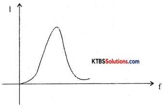
As the frequency of AC source is increased, the capacitive reactance of the capacitor decreases and .inductive reactance of the .inductnr increases . The values of X1 and Xc will be same at resonance frequency fr.
XL =Xc
2πfrL = \(\frac{1}{2 \pi f_{\mathrm{r}} C}\)
4π2fr2LC = 1
fr2 = \(\frac{1}{4 \pi^{2} L C}\)
fr = \(\frac{1}{2 \pi \sqrt{\mathrm{LC}}}\)
The current in RLC circuit will be maximum at resonance the variation of current with frequency is as shown below:
(b) Draw the circuit diagram and frequency response curve of RC high pass filter. (2M)
Answer:
A high pass filter passes all high frequencies above cut-off and rejects the lower frequencies.
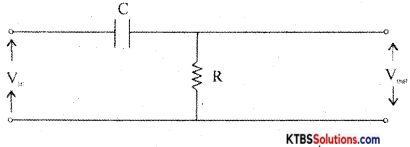
At low frequencies, capacitor acts as open circuit (∴ Xc = \(\frac{1}{2 \pi \mathrm{RC}}\) = HIGH) At high frequencies, the capacitor acts as a short circuit. Hence all the input appears the output resistor. The cut off frequency, fc = \(\frac{1}{2 \pi \mathrm{RC}}\)
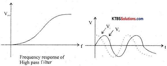
As the output voltage leads the input voltage, the high pass filter is also called a lead network.
![]()
Question 36.
(a) What is a clipping circuit?
(b) With the help of circuit diagram and input-output waveforms, explain the working of positive diode clamper (4M)
Answer:
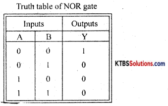
Question 37.
With a circuit diagram and truth, the table explains the working of two input DTL NOR gates.
Answer:
NOR gate is a logic circuit whose output is HIGH only when both its inputs are LOW
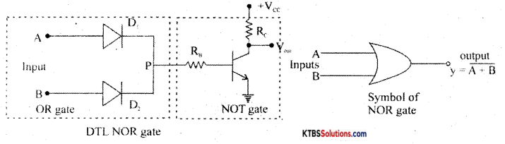
Diodes D1 and D2 form OR gates and the transistor act as NOT gate.
Case (1) When A = 0, B = 0, the diodes are not forward biased and they do not conduct. Hence voltage P is zero. This zero voltage makes the transistor go to cut-off condition and therefore output is HIGH.
Case (ii) When A = 0, B = 1, D1 does not conduct but D2 conducts. Hence voltage at P is +Vcc and it drives the transistor to saturation and output becomes LOW.
Case (iii) When A = 1, B = 0, D1 conducts and D2 does not conduct. Hence voltage at P is +Vcc and this makes the transistor Q go to saturation. Hence output becomes LOW.
Case (iv) When A = 1, B = 1, both diodes conduct as they are forward biased. Then voltage at P is +Vcc and the transistor is dñvcn to saturation. The output at the collector becomes LOW.