Students can Download 1st PUC Electronics Previous Year Question Paper March 2018 (North), Karnataka 1st PUC Electronics Model Question Papers with Answers helps you to revise the complete syllabus.
Karnataka 1st PUC Electronics Previous Year Question Paper March 2018 (North)
Time: 3.15 Hours
Max Marks: 70
Instructions:
- The question paper contains four parts.
- Part – A is compulsory,
- Part – D contains two subparts (i) Problems and (ii) Essay-type questions.
- Draw circuit diagrams wherever necessary
PART-A
Answer ALL questions: (10 × 1 = 10)
Question 1.
Expand IGBT.
Answer:
IGBT = Insulated Gate Bipolar junction Transistor.
Question 2.
Write the unit of frequency.
Answer:
Hertz (Hz).
Question 3.
Draw the symbol of the cell.
Answer:
![]()
Question 4.
What is the principle of a transformer?
Answer:
Mutual Induction.
Question 5.
Under what bias condition is a varactor diode operated.
Answer:
Reverse Bias.
![]()
Question 6.
Which impurity is added to form an n-type semiconductor.
Answer:
Phosphorous / Arsenic / Antimony.
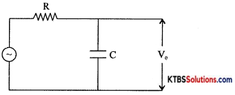
Question 7.
Draw the circuit diagram of the low pass filter.
Answer:
Question 8.
How many junctions are there in a transistor?
Answer:
Two junctions
Question 9.
Convert (AB)16 to binary number.
Answer:
(AB)16=(1010 1011)2.
Question 10.
Mention any one specification of a capacitor.
Answer:
Value of capacitance or voltage rating.
PART-B
Answer any FIVE questions. (5 × 2 = 10)
Question 11.
Name any two fixed resistors.
Answer:
Carbon composition resistor, Wire-wound resistor.
Question 12.
What is a DC ammeter? Draw its symbol.
Answer:
Meter used to measure DC current is called DC ammeter.
![]()
Question 13.
What is the ultrasound scan?
Answer:
An ultrasound scan uses sound waves to create images of organs inside the body.
![]()
Question 14.
Derive an expression for resonance frequency in LCR series circuit
Answer:
XL = Xc
2πfL = \(\frac{1}{2 \pi f c}\)
f = \(\frac{1}{2 \pi \sqrt{L C}}\)
Question 15.
Determine the reactance of 5 mH of the inductor connected to ac of 230 V, 100 Hz.
Answer:
XL = 2πfL = 2(3.14)(100)(5 × 10⁻³)
XL = 3.14Ω
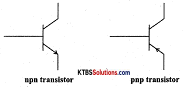
Question 16.
Draw the symbol of npn and pnp transistor.
Answer:
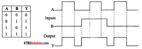
Question 17.
Write the truth table and timing diagram of the two-input OR gate.
Answer:
Question 18.
Mention any two advantages of PCB.
Answer:
- The circuit becomes compact and simple.
- PCB can be tested by a computer.
PART-C
Answer any FIVE questions. (5 × 3 = 15)
Question 19.
Write a note on the scope of electronics.
Answer:
Electronics engineers are employed in the design and development of complex devices and systems for signal processing and telecommunication in defense, space, and other large research organizations.
Electronics engineers find job opportunities in the design and fabrication of devices, integrated circuits, embedded systems. Electronics technicians have jobs in the installation and maintenance of electronic equipment used in health care in hospitals, equipment for instruments.
![]()
Question 20.
State Ohm’s law. Write any two limitations of Ohm’s law.
Answer:
Ohms law states that the current flowing through a conductor is directly proportional to the potential difference across the conductor when the temperature and other physical conditions of the conductor are maintained constant.
- Ohms law is not valid when the physical conditions of the conductor change.
- Ohms law is not valid at very low and very high temperatures.
Question 21.
Calculate the effective resistance between A & B.
i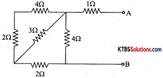
Answer:
RS = R1 + R2 = 2 + 4 = 6Ω
Rp = (6) ∥ (3) = \(\frac{R_{1} R_{2}}{R_{1}+R_{2}}=\frac{6 \times 3}{6+3}\) = 2Ω
Rs = R1 + R2 = 2 + 2 = 4Ω
Rp = (4) ∥ (4) = \(\frac{\mathrm{R}_{1} \mathrm{R}_{2}}{\mathrm{R}_{1}+\mathrm{R}_{2}}=\frac{4 \times 4}{4+4}\) = 2Ω
REff = Rs = R1 + R2 = 2 + 1 = 3Ω
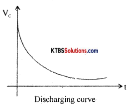
Question 22.
With circuit diagram and phasor diagram show the relation between voltage and current when ac is applied to a capacitive network.
Answer:
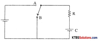
When the switch is in position A, the capacitor gets charged. When the switch is in position B, the capacitor starts getting discharged through the resistor R. The voltage across the capacitor decreases and ¡t takes infinite time to get discharged completely. Discharging voltage across the capacitor at a time after the switch is input in the position B is, V = V0e-1/RC
The time constant can be defined as the time taken by the capacitor to discharge to 36.8% of its maximum voltage.
Question 23.
Write the properties of semiconductors.
Answer:
- Semiconductors are tetravalent and hence covalent bonding takes place between their atoms.
- At absolute zero, semiconductors behave like a perfect insulator.
- Resistance of semiconductors decreases when their temperature is increased (α the temperature coefficient of resistance is negative)
- The conductivity of semiconductors can be increased by adding suitable impurities to them.
![]()
Question 24.
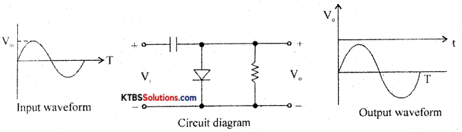
What is a positive clamper? Draw the circuit diagram with input and output waveform.
Answer:
A negative clamper is a circuit that clamps the negative peak of a signal to a desired de level.
Question 25.
What is a phototransistor? Write its application
Answer:
A phototransistor is a three-terminal optoelectronics device.
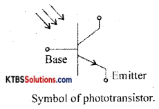
Applications:
- optocouplers
- fire alarms
- Counting systems
- Lighting controls in high ways.
Question 26.
Prove that A + BC = (A + B) (A+ C)
Answer:
R.H.S = (A + B) (A + C)
= A.A + AC + B.A + BC
= A + AC + BA + BC {∵ A.A = 1}
= A(1 + C) + AB + BC
= A.1 +AB + BC {∵ 1 + C = 1}
= A + AB + BC {∵A.1 = A}
= A(1 + B) + BC
= A. 1 + BC {∵ A.1 = A}
= A + BC
= L.H.S
PART-D
Answer any THREE questions: (3 × 5 = 15)
Question 27.
Determine the current through RL using Thevenin’s theorem.
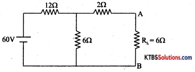
Answer:
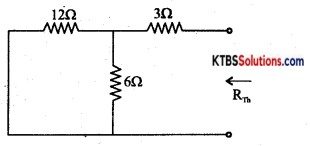
RTh = (12) ∥ (6) = \(\frac{R_{1} R_{2}}{R_{1}+R_{2}}=\frac{12 \times 6}{12+6}\) = 4Ω
RT = Rs = R1 + R2 = 4 + 2 = 6Ω
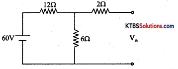
VTh = \(\frac{6 \times 6}{6+12}\) = 20V
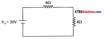
IL = \(\frac{\mathrm{V}_{\mathrm{Th}}}{\mathrm{R}_{\mathrm{Th}}+\mathrm{R}_{\mathrm{L}}}=\frac{20}{6+4}\) = 2A
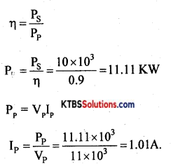
Question 28.
A step-down transformer having a power output of 10 kW and efficiency of 90% reduces the voltage from 11 kV to 220V. Calculate
(i) number of turns in the primary if the secondary has 100 turns.
(ii) the current in the primary.
Answer:
Question 29.
A 10Ω resistance in series with XL = 80Ω and Xc = 60Ω the applied voltage is 50 mV with a frequency of 50 Hz. Calculate Impedance (Z), current (I), and phase angle (Φ).
Answer:
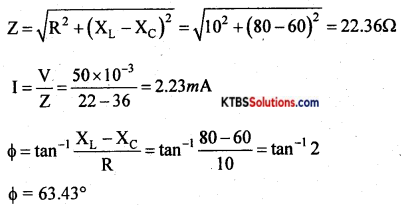
![]()
Question 30.
A half-wave rectifier uses a diode with a forward resistance of 50Ω. If input ac voltage is 200 Vrms and the load resistance of 1KW. Determine
(i) Im Idc and Irms (ii) PIV (iii) DC output power
Answer:
Vm = \(\sqrt{2}\) = Vrms = 260 × \(\sqrt{2}\) = 282.84 V
Im = \(\frac{\mathrm{V}_{m}}{\mathrm{R}_{\mathrm{L}}+\mathrm{R}_{\mathrm{F}}}=\frac{282.5 \mathrm{~V}}{1 \times 10^{3}+50}\) = 0.269 A
Idc = \(\frac{\mathrm{I}_{m}}{\pi}=\frac{0.269}{3.14}\) = 0.086 A
Irms = \(\frac{\mathrm{I}_{m}}{\sqrt{2}}=\frac{0.269}{1.414}\) = 0.19 A
PIV = Vm = 282.84 V
P0 = I2rms RL = (0.19)2 × 1 × 103
P0 = 0.0361kW
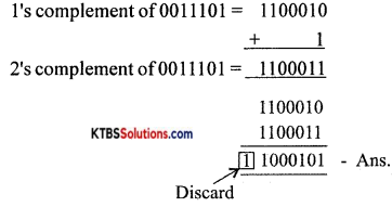
Question 31.
Subtract (29)10 from (98)10 using 2’s complement method.
Answer:
(98)10= 1100010
(29)10 = 0011101
PART-E
Answer any FOUR questions. . (4 × 5 = 20)
Question 32.
State and explain the maximum power transfer theorem.
Answer:
In any linear bilateral network consisting of two or more independent sources, the resultant current or voltage in any branch is the algebraic sum of the currents or voltages caused by each independent source acting alone, with all other independent sources being replaced by their internal resistances.
Procedure for using Superposition Theorem:
Step 1: Retain the source V1 and replace all other sources with their internal resistances.
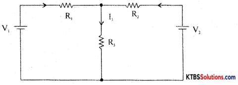
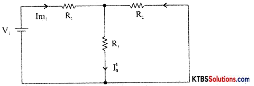
Step 2: Current in various branches and their voltage drops due to V1 alone are determined as follows,
RT1 = R1 + \(\frac{\mathrm{R}_{2} \mathrm{R}_{3}}{\mathrm{R}_{2}+\mathrm{R}_{3}}\)
Im1 = \(\frac{\mathrm{V}_{1}}{\mathrm{R}_{\mathrm{T}_{1}}}\)
I’3 = Im1 × \(\frac{R_{2}}{R_{2}+R_{3}}\) {from branch current formula}
Voltage across R3 = V’3 = I’3 = I”1 = Im2 × \(\frac{R_{1}}{R_{1}+R_{3}}\)
Step 3 : Consider V2 alone and find the currents and voltages as follows:
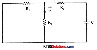
RT2 = R2 + \(\frac{\mathrm{R}_{1} \mathrm{R}_{3}}{\mathrm{R}_{1}+\mathrm{R}_{3}}\)
Im2 = \(\frac{\mathrm{V}_{2}}{\mathrm{R}_{\mathrm{T}_{2}}}\)
I”3 = V2 × \(\frac{\mathrm{R}_{1}}{\mathrm{R}_{1}+\mathrm{R}_{3}}\)
Step 4: Find the algebraic sum of currents and voltage drops in a branch.
I3 = I’3 + I”3; V’3 = I’3R3, V = I”3R3
V3 = V’3 + V”3
Question 33.
Explain constructional features of metal film resistors.
Answer:
A mixture of finely divided carbon and a powdered insulating material forms the resistor element. The mixture is molded into a cylindrical shape. The proportion of the mixture is adjusted to get the desired value of resistance. Metal caps with leads of tinned copper wire are joined to two ends of a carbon-coated resistor for external connection. As the leads are joined axially from the ends, they are called axial leads. The non-conductive material is coated on the resistor element for insulation and mechanical strength. To specify the resistance of the resistor, a band of colors is marked on the body of the resistor.
Carbon composition resistors are smaller in size and cheap. They are available in the resistance range of 1Ω to 20MΩ. Their power rating is \(\frac{1}{10}, \frac{1}{8}, \frac{1}{4}, \frac{1}{2}\)1 and 2w. These resistors are used where accuracy is not important.
Question 34.
Define the following terms with respect to an AG signal
(a) cycle
Answer:
The frequency of AC is the number of AC cycles completed in one second.
(b) effective value
Answer:
The peak value of AC is the maximum voltage or current of the ac in its one of half cycles.
(c) peak to peak value
Answer:
The peak to the peak value of AC is the maximum value attained in both positive and negative half cycles of AC.
(d) average value
Answer:
RMS value of ac is the equivalent steady DC value which gives the same heating effect as the same rate in a given resistor.
![]()
Question 35.
Classify solids based on the energy band diagram.
Answer:
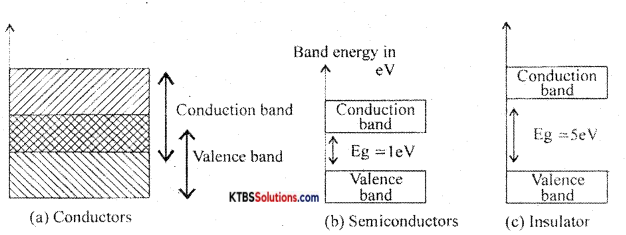
Conductors: These are materials that allow the current to flow through them easily. In conductors, the valence band and conduction band overlap completely due to which the valence electrons drift to the conduction band easily. Even at room temperature, there is a large number of free electrons. Hence due to the small voltage applied a large current flows through them.
Semiconductors: These are the materials with electrical conductivity lying between those of conductors and insulators. The forbidden energy gap between the valence band and conduction band is 0.7 eV for germanium and I. I eV for silicon. At absolute zero, a semiconductor acts as an insulator. As the temperature increases, more valence electrons jump to the conduction band. Hence the conductivity of semiconductors increases with an increase in their temperature.
Insulators: Insulators are materials that do not allow the electric current to flow through them easily. The valence band is completely filled and the conduction band ¡s completely empty in insulators. The forbidden energy band between the conduction band and valence band ¡s nearly 5eV. In the conduction band, there are no free electrons present at room temperature. Hence, the insulators do not conduct at all at room temperature.
Question 36.
Explain the working of the Zener diode, a voltage regulator.
Answer:
In a DC power supply. the output voltage should remain almost constant even as the input and load vary.
Voltage regulation is a measure of the ability of a DC source to maintain a constant output voltage, even whén there is variation in the load resistance or input voltage.
Zener diode as a voltage regulator
Zener diode can be used as a voltage regulator to provide a constant output voltage from a source whose voltage may vary.
The two types of voltage regulator are
- Line regulation
- Load regulation.
Load regulation :
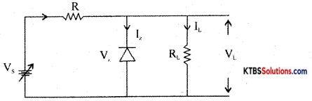
The Zener diode starts conducting only when the source voltage V is greater than Zener breakdown voltage V.
When V is increased from 0V, load current VL increases with applied voltage. The current through Zener diode will be zero.
If V is more than V, the Zener dioðe breaks down and conducts. Increasing the input voltage further increases voltage across the resistor R and voltage across load VL remains constant at V.
Line regulation :
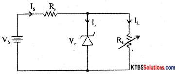
For load regulation, VL is made greater than V. VL is kept constant and load resistance R. is varied. If RL is decreased, current VL increases and 1 decreases by the same value, but output voltage VL = V remains constant.
If RL is increased, VL decreases and IL increases, but output voltage VL = V remains constant.
Question 37.
Explain with the DTL logic circuit the working of the two-input NAND gate.
Answer:
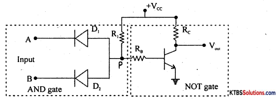
Case (i) When both inputs A and B are LOW (0V), both the diodes D1 and D2 are forward biased. Hence voltage at junction P of the diode becomes zero. This makes the transistor Q go to cut off. Hence the output at the collector of the transistor becomes HIGH.
Case (ii) When A is LOW and B is HIGH, D1 is forward biased and D2 ¡s reverse biased. Hence the voltage at P becomes zero. This makes the transistor go to a cut-off state and therefore output at its collector becomes HIGH.
Case (iii) When A is HIGH and B is LOW, D1 ¡s reverse biased, and D2 is forward biased due to which voltage at P is zero. This makes the transistor go to cut off state and therefore output at its collector becomes HIGH,
Case (iv) When both the inputs are HIGH, D1 and D2 are reverse biased. Hence voltage at P becomes This makes the transistor Q go to saturation and the transistor acts like a closed switch. Therefore output becomes LOW.