Students can Download 1st PUC Electronics Previous Year Question Paper March 2018 (South), Karnataka 1st PUC Electronics Model Question Papers with Answers helps you to revise the complete syllabus.
Karnataka 1st PUC Electronics Previous Year Question Paper March 2018 (South)
Time: 3.15 Hours
Max Marks: 70
Instructions:
- The question paper contains four parts.
- Part – A is compulsory,
- Part – D contains two subparts (i) Problems and (ii) Essay-type questions.
- Draw circuit diagrams wherever necessary
PART-A
Answer ALL questions. (10 × 1 = 10)
Question 1.
Expand IGBT.
Answer:
IGBT = Insulated Gate Bipolar junction Transistor.
Question 2.
Write the unit of electric charge.
Answer:
Coulomb.
Question 3.
What is a ‘loop’ in an electrical circuit?
Answer:
A loop is any closed path in an electrical circuit.
Question 4.
Draw the circuit symbol of the potentiometer.
Answer:
![]()
Question 5.
Mention anyone pressure transducer.
Answer:
Microphone or Loudspeaker.
![]()
Question 6.
Name any one donor impurity.
Answer:
Arsenic, or Phosphorous or Antimony.
Question 7.
Draw the symbol of a varactor diode.
Answer:
![]()
Question 8.
Mention the heavily doped region of a transistor.
Answer:
Emitter
Question 9.
Write the l’s complement of (101101)2.
Answer:
(010010)2.
Question 10.
Name the type of capacitor having polarity.
Answer:
Electrolytic capacitor.
PART-B
Answer any FIVE questions. (5 × 2 = 10)
Question 11.
Mention any four controls of an oscilloscope.
Answer:
(i) Intensity control
(ii) Contrast control (Focus)
(iii) Volt/division control
(iv) Ampere / division
Question 12.
Write any two advantages of an ultrasound scan.
Answer:
- Ultrasound scan detects abnormalities of heart structure.
- To monitor abnormalities of the unborn child.
Question 13.
Distinguish between tweeter and woofer.
Answer:
Woofers are speakers to reproduce low frequencies and tweeters are speakers to reproduce high frequencies.
![]()
Question 14.
What is the resistance value of SMD resisotr: (a) ‘223’ (b) ‘4R7’.
Answer:
(a) 223 = 22 × 103Q = 22 kΩ.
(b) 4R7 = 4.7Ω.
Question 15.
Define the time constant of the RC circuit and write its expression.
Answer:
The time constant of the RC circuit is the time taken by the voltage across the capacitor to become 63.2% of the supply voltage.
Question 16.
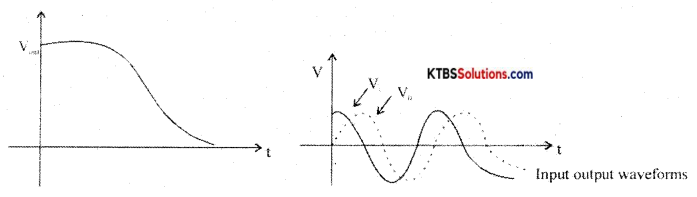
Draw the circuit diagram of the low pass filter and high pass filter.
Answer:
Low pass filter:
The low pass filter passes all the low frequencies below a cutoff frequency and stops or attenuates the higher frequencies.
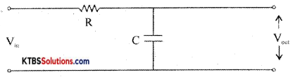
The input is applied across the RC circuit and the output is taken across the capacitor.
At low frequencies, the capacitive reactance Xc = \(\frac{1}{2 \pi \mathrm{fc}}\) is high and hence entire input voltage appears across the output. At high frequencies, the capacitor offers very low reactance and acts as a short circuit and hence output becomes Zero. The cut off frequency fc = \(\frac{1}{2 \pi \mathrm{Rc}}\)
High pass filter:
A high pass filter passes all high frequencies above cut-off and rejects the lower frequencies.
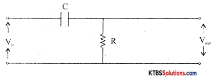
At low frequencies, capacitor acts as open circuit (∴ X = \(\frac{1}{2 \pi \mathrm{RC}}\) = HIGH) At high frequencies, the capacitor acts as a short circuit. Hence all the input appears the output resistor. The cut off frequency, fc = \(\frac{1}{2 \pi \mathrm{RC}}\)
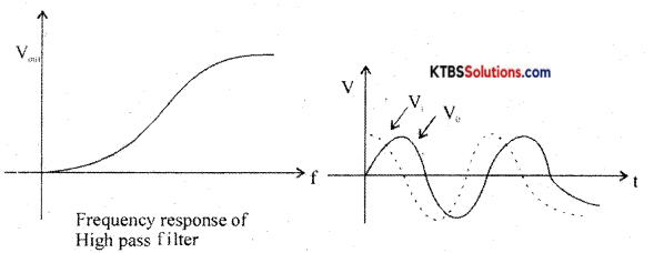
As the output voltage leads the input voltage, the high pass filter is also called a lead network.
Question 17.
Write the properties of semiconductors.
Answer:
- Semiconductors are tetravalent and hence covalent bonding takes place between their atoms.
- At absolute zero, semiconductors behave like a perfect insulator.
- Resistance of semiconductors decreases when their temperature is increased (the temperature coefficient of resistance is negative)
- The conductivity of semiconductors can be increased by adding suitable impurities to them.
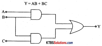
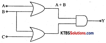
Question 18.
Draw the logic diagram for the following Boolean expression
(a) y = AB + BC
(b) y = (A + B) (B + C)
Answer:
Y = AB + BC
Y = (A+B)(B + C)
PART-C
Answer any FIVE questions. (5 × 3 = 15)
Question 19.
Give a brief note on the scope of electronics.
Answer:
Question 20.
State and explain ohm’s law.
Answer:
Ohms law states that the current flowing through a conductor is directly proportional to the potential difference across the ends of the conductor.
If I is the current through the conductor and V is the potential difference, then
I ∝ V
I = \(\frac{V}{R}\)
or V = IR
Question 21.
Find the resistance between A and B.
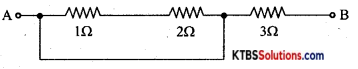
Answer:
\(\frac{1}{\mathrm{R}_{\mathrm{P}}}=\frac{1}{\mathrm{R}_{1}}+\frac{1}{\mathrm{R}_{2}}+\frac{1}{\mathrm{R}_{3}}\)
\(\frac{1}{R_{P}}=\frac{1}{1}+\frac{1}{2}+\frac{1}{3}=\frac{11}{6}\)
Rp= \(\frac{6}{11}\) = 0.54Ω
![]()
Question 22.
Explain the construction of wire wound resistors.
Answer:
Wire wound resistor is made by winding a wire of known length on a hollow porcelin tube. Eureka wire, an alloy of 60% nickel and 40% copper, is used as a resistance wire. Tinned copper leads are attached to the ends of the winding for connection. The entire assembly is covered with a protective insulation coating of porcelain. The length, thickness, and specific resistivity of the resistance wire determine the resistance value. Their resistance varies from 1Ω to 1000Ω. They are available with a power rating from 5W to 100W. Wire wound resistors have good stability, reliability, and high power ratings. The resistance value and the power ratings are printed on the body of the resistance. These resistors are used in audio frequency applications.
Question 23.
Derive an expression for resonant frequency of a series resonant circuit.
Answer:
At resonance, Xc = XL
2πfL = \(\frac{1}{2 \pi \mathrm{fL}}\)
f2 = \(\frac{1}{4 \pi_{2} \mathrm{LC}}\)
f = \(\frac{1}{2 \pi \sqrt{L C}}\)
Question 24.
For a Zener diode voltage regulator with Vs = 20V, Rs = 100Ω, Vz = 12V, RL = 680Ω. Determine (a) Load voltage (b) Voltage drop across series resistance (c) Current through the series resistance.
Answer:
VL = Vz = 12 V
VRS = VL – Vz = 20 – 12 = 8V
IRS = \(\frac{\mathrm{V}_{\mathrm{RS}}}{\mathrm{I}_{\mathrm{RS}}}=\frac{8}{100}\) = 0.08 = 80mA
Question 25.
Define (a) Bit (b) Nibble (c) Byte with respect to the binary number system.
Answer:
(a) A bit is a binary digit, the smallest increment of data on a computer. A bit can hold only one of two values: 0 or 1, corresponding to the electrical values of off or on, respectively.
(b) a nibble (occasionally nybble or nybble to match the spelling of byte) is a four-bit aggregation or half an octet. It is also known as half-byte or trade.
(c) a byte is a unit of data that is eight binary digits long. A byte is a unit most computers use to represent a character such as a letter, number, or typographic symbol. Each byte can hold a string of bits that need to be used in a larger unit for application purposes.
![]()
Question 26.
Write the steps involved in PCB designing.
Answer:
PCB layout preparation: PCB layout must be drawn using PC. The complete circuit must be drawn on paper. Prepare computer layout as per circuit diagram using PCB design software.
Draw tracks for connecting one component to the other. Take printout on a white sheet and get the film done on a transparent sheet by filmmakers.
Photoresist: Photoresist film or mask is placed on a copper clad board. UV light is exposed on a copper-clad board covered by photoresist film. UV light does not pass through the photoresist on the tracks. The copper area which is not covered protected by photo-resist is removed during the etching process.
PCB etching process: The etching process is done to remove the unnecessary copper after UV exposure, leaving behind only the desired copper tracks. The PCB is then dipped in fern chloride or hydrochloric acid until unwanted copper is dissolved.
Then the PCB is dipped in acetone to remove the black color giving the PCB a shining attractive look.
PCB Drilling: The components to be attached to PCB can be done only by vias drilling le, by drilling a hole. To make PCB good solderable the surface of the PCB is coated with tin or nickel.
PCB assembling: The electronic components are assembled on the respective holes in the PCB. The component leads are electrically and mechanically fixed to the board with solder.
PART-D
Answer any THREE questions: (3 × 5 = 15)
Question 27.
Find the value of load RL in fig, for the maximum power to be transferred and calculate the maximum power transferred to the load.
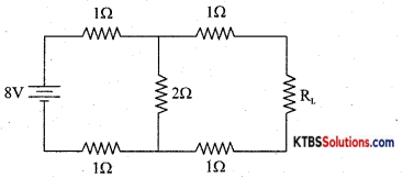
Answer:
RL = RTh = {(1 + 1) ∥ 2} + 1 + 1 = 3Ω
VTh = \(\frac{8 \times 2}{2+1+1}\) = 4V
PL(max) = \(\frac{\mathrm{V}_{\mathrm{Th}}^{2}}{4 \mathrm{R}_{\mathrm{Th}}}\) = 1.33W
Question 28.
(a) An iron core length of 20 × 102m and area of cross-section 3 × 10⁻⁴ m2 is wound with a coil of 200 turns. Over this coil is wound another coil of 250 turns. The relative permeability of iron is 800. Determine the mutual inductance between the two coils. (3M)
Answer:
M = \(\frac{\mu_{0} \mu_{r} \mathrm{~N}_{1} \mathrm{~N}_{2} \mathrm{~A}}{l}=\frac{4 \pi \times 10^{-7} \times 800 \times 200 \times 250 \times 3 \times 10^{-4}}{20 \times 10^{-2}}\) = 90μJ
(b) Find the energy stored ¡n a 5H inductor when a current of 6mA is flowing through it. (2M)
Answer:
E = \(\frac{1}{2}\) LI2 = \(\frac{1}{2}\) × 5 × (6 × 10-3)2 = 90μJ
Question 29.
Determine the time constant, the current through an inductor during the growth at t = 1s in a DC circuit containing R = 1W and L = 1H connected to a DC supply of 20V.
Answer:
τ = \(\) = 1S
I0 = \(\) = 20A
I = I0[1 – e-(R/L)t] = 20[1 – e-1] = 20[1 – \(\frac{1}{e}\)] = 20[1 – 0.368] = 12.64A
![]()
Question 30.
A 230V, 50Hz AC voltage is applied to the primary 5:1 step-down transformer, which is used in the bridge rectifier, having a local resistance of 100. Assuming the diodes to be ideal, determine (a) DC output current (b) DC output voltage (c) DC power delivered to the load.
Answer:
Vrms = Vs = \(\frac{\mathrm{N}_{\mathrm{S}}}{\mathrm{N}_{\mathrm{P}}}\) × Vp = \(\frac{1}{5}\) × 230 = 46V
Vm = Vrms × \(\sqrt{2}\) = 65.05V
Idc = \(\frac{2 V_{m}}{\pi R_{L}}\) = 0.41A
Vdc = \(\frac{2 V_{m}}{\pi}\) = 41.4V
Pdc = I2dc × RL = 16.8W
Question 31.
(a) Subtract (10110) from (101001)2 using 2’s complement method. (3M)
Answer:
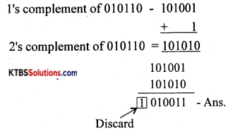
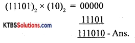
(b) Multiply: (11101) × (10). (2M)
Answer:
Answer any FOUR questions (4 × 5 = 20)
Question 32.
Define the following terms: (a) cycle (b) Time period (c) Frequency (d) RMS value (e) Average value for on AC signal.
Answer:
(a) Frequency of AC is the number of AC cycles completed in one second.
(b) Time period of AC is the time taken to complete one cycle.
(c) Peak value of AC is the maximum voltage or current of the ac in its one of half cycles.
(d) RMS value of ac is the equivalent steady DC value which gives the same heating effect as the same rate in a given resistor.
(e) Peak to the peak value of AC is the maximum value attained in both positive and negative half cycles of AC.
Question 33.
(a) Derive an expression for the equivalent capacitance of two capacitors connately in parallel. (3M)
Answer:
Capacitors are said to be in parallel if they are connected between the same common points.
The voltage across each capacitor in parallel is the same.
Let C1, C2, and C3 be the capacitors connected in parallel.
Let V be the applied voltage across the combination.
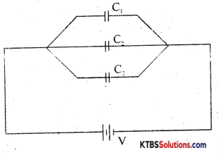
The charge Q from the cell equals the sum of voltages across the capacitors.
Q = Q1 + Q2 + Q3
= C1V + C2V + C3V
Q = V(C1 + C2 + C3) →(1)
The equivalent or effective capacitor is a single capacitor that has the same effect as the combination of capacitors.
If Cp is the effective capacitance then
Q = CpV→(2)
From equations (1) and (2)
CpV = V(C1 + C2 + C3)
Cp = C1 + C2 + C3
Hence, when capacitors are connected in series, the effective capacitance is the sum of individual capacitances.
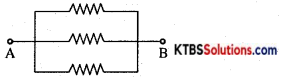
(b) What do you mean by open and short circuits? (2M)
Answer:
An open circuit is a discontinuity in the circuit in which the current is zero. A short circuit is a continuity in the circuit due to which maximum current flows.
![]()
Question 34.
Classify solids based on the energy band diagram.
Answer:
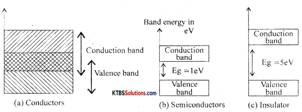
Conductors: These are materials that allow the current to flow through them easily. In conductors, the valence band and conduction band overlap completely due to which the valence electrons drift to the conduction band easily. Even at room temperature, there is a large number of free electrons. Hence due to the small voltage applied a large current flows through them.
Semiconductors: These are the materials with electrical conductivity lying between those of conductors and insulators. The forbidden energy gap between the valence band and conduction band is 0.7 eV for germanium and 1. 1 eV for silicon. At absolute zero, a semiconductor acts as an insulator. As the temperature increases, more valence electrons jump to the conduction band. Hence the conductivity of semiconductors increases with an increase in their temperature.
Insulators: Insulators are materials that do not allow the electric current to flow through them easily. The valence band is completely filled and the conduction band is completely empty in insulators. The forbidden energy band between the conduction band and valence band is nearly 5eV. ¡n conduction band, there are no free electrons present at room temperature. Hence, the insulators do not conduct at all at room temperature.
Question 35.
Explain the working of half-wave rectifier with circuit diagram and input, output waveform.
Answer:
Half wave rectifier is a circuit that removes one-half cycle of the AC input and produces a pulsating DC output voltage.
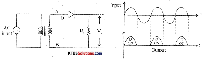
It has diode D in series with a load resistor RL. The AC mains voltage to be rectified is applied to the primary of a transformer and voltage induced across secondary is applied to the rectifier.
During the positive half cycle, A ¡s positive and B is negative. The diode is forward biased and conducts and the diode acts as a closed switch. Hence, the positive half cycle of the voltage is developed across the load resistor RL.
During the negative half-cycle, A is negative and B is positive. The diode is reverse biased and does not conduct as it acts as an open switch. Hence there is no output. The output waveform across RL has only positive half cycles. Ripple factor ¡s the ratio of RMS value of(r) the AC component of the load voltage to the average value of load voltage.
r = \(\frac{\text { rms value of AC component }}{\text { value of dc component }}\) = 1.21
Rectifier efficiency is the ratio of de output power to ac input power.
η = \(\frac{\text { DC output power }}{\text { AC input power }}\) = 0.406 or 40.6%
Peak inverse voltage is the maximum voltage the diode can withstand when ¡t is reverse biased and is equal to the peak value of the secondary voltage Vm.
Question 36.
Explain CE mode output characteristics of an NPN transistor and explain cut-off, saturation, and the active region.
Answer:
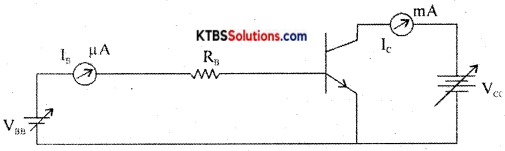
The circuit to plot the CE characteristics of the transistor is as shown in the diagram.
The two types of characteristics are :
- Input characteristics.
- Output characteristics.
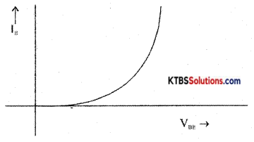
Input Characteristics:
It gives the relationship between input voltage VBE and the input current Is when the output voltage VCE is kept constant. VBE is varied and corresponding VBE values are noted keeping VCE constant. The input characteristics curve ¡s similar to that of a forward-biased semiconductor diode as emitter-base junction a pn junction.
Input resistance Rm = \(\frac{\Delta \mathrm{V}_{\mathrm{BE}}}{\Delta \mathrm{I}_{\mathrm{B}}}\)
CE output characteristics
It is a graph of output collector current Ic against output collector to emitter voltage VCE for a constant input base current IB.
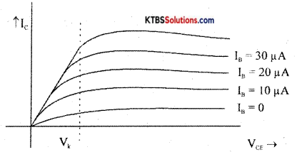
From the graph, it is clear that the output current IB depends upon input current IB, and VCE has no control over Ic.
Output resistance, Rout = \(\frac{\Delta \mathrm{V}_{\mathrm{CE}}}{\Delta \mathrm{I}_{\mathrm{C}}}\)
![]()
Question 37.
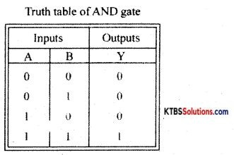
(a) What is AND gate? Draw its symbol and truth table for 2 input AND gate. (3M)
Answer:
AND gate is a logic gate that produces a HIGH output only when all its inputs are HIGH.
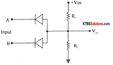
Working:
Case (1) When A = 0, B = 0, both the diodes are forward biased and act like closed switches. Hence all the applied voltage drops across R1 and the output voltage becomes LOW.
Case (ii) When A = 0, B = 1, diode D1 conducts as it is forward biased and diode D2 does not conduct as it is reverse biased. Hence all the applied voltage drops across R1 and the output voltage becomes LOW.
Case (iii) When A= 1, B = 0, diode D1 does not conduct but D2 conducts being forward biased. Hence all the applied voltage drops across R1 and the output voltage at y becomes LOW.
Case (iv) When A = 1, B = 1 both diodes are reverse biased and do not conduct. No current flows through R and hence no voltage drop across R. Hence output at y becomes HIGH.
(b) Simplify the given boolean expression: y = AB + A(\(\overline{(B+C)}\)). (2M)
Answer:
y = AB + A(\(\overline{(B+C)}\))
= AB + A(B̅.C̅)
= A[B + \(\overline{\mathrm{BC}}\)]
= A[B + C̅]
= AB + AC̅