Students can Download 1st PUC Electronics Previous Year Question Paper March 2019 (North), Karnataka 1st PUC Electronics Model Question Papers with Answers helps you to revise the complete syllabus.
Karnataka 1st PUC Electronics Previous Year Question Paper March 2019 (North)
Time: 3.15 Hours
Max Marks: 70
Instructions:
- The question paper contains four parts.
- Part – A is compulsory,
- Part – D contains two subparts (i) Problems and (ii) Essay-type questions.
- Draw circuit diagrams wherever necessary
PART-A
Answer ALL the following questions: (10 × 1 = 10)
Question 1.
Who invented integrated circuits?
Answer:
Jack Kilby.
Question 2.
Define potential differences.
Answer:
The difference of electrical potential between two points,
Question 3.
Expand E.C.GL
Answer:
Electrocardiogram.
Question 4.
Name the advice which gathers the data concerning the temperature from a source.
Answer:
Thermistor.
![]()
Question 5.
What is the unit of impedance?
Answer:
Ohm.
Question 6.
Determine ID for the circuit shown below.
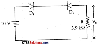
Answer:
0A
Question 7.
Mention the value of the ripple factor of HWR.
Answer:
1.21.
Question 8.
How many ‘pn’ junctions a transistor has?
Answer:
Two.
![]()
Question 9.
What is a byte?
Answer:
A byte is 8 bits.
Question 10.
Write the part number for the diode.
Answer:
IN 4007.
PART-B
Answer any FIVE of the following questions. (5 × 2 = 10)
Question 11.
Mention any two properties of charges.
Answer:
- as charges repel, unlike charges, attract.
- Charges always reside on the outer surface of a conductor only.
Question 12.
Find the resistance between A & B.
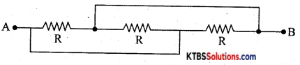
Answer:
\(\frac{1}{\mathrm{R}_{\mathrm{P}}}=\frac{1}{\mathrm{R}_{1}}+\frac{1}{\mathrm{R}_{2}}+\frac{1}{\mathrm{R}_{3}}\)
\(\frac{1}{\mathrm{R}_{\mathrm{P}}}=\frac{1}{\mathrm{R}}+\frac{1}{\mathrm{R}}+\frac{1}{\mathrm{R}}=\frac{3}{\mathrm{R}}\)
Rp = \(\frac{\mathrm{R}}{3}\)
Question 13.
Write any two applications of an oscilloscope.
Answer:
The oscilloscope can be used to measure
- current
- voltage
- time period and
- frequency.
![]()
Question 14.
Name the factors on which the inductance of a coil depends.
Answer:
Self-inductance of a coil depends on
- number of turns in the coil
- length of the coil
- relative permeability of the coil
- The cross-sectional area of the coil.
Question 15.
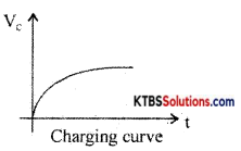
Discuss the charging of a capacitor in an RC circuit.
Answer:
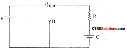
Consider a resistor R and a capacitor C connected in series with a battery of emf E. When the switch is in position A, the capacitor C gets charged through R exponentially with time. Hence Voltage across the capacitor increases èxponentially and the current in the circuit decreases exponentially. When the capacitor is fully charged, the current becomes Zero. The instantaneous value of voltage across the capacitor during charging is given by
V = V0(1 – e1/RC)
The instantaneous value of current is I = I0e1/RC Time constant (τ) of an RC circuit is the time taken by the capacitor to charge to 63.2% of maximum current.
Question 16.
Mention majority and minority charge carriers in n-type semiconductors.
Answer:
The majority of charge carriers in n-type semiconductors are electrons and the minority charge carriers are holes.
Question 17.
A transistor amplifier connected in CE mode has β = 100 ad IB = 50 mA. Calculate the value of Ic and oc.
Answer:
Ic = βIB = 100 × 50 × 10-6 = 5 mA
α = \(\frac{\beta}{\beta+1}=\frac{100}{100+1}=\frac{100}{101}\)
α = 0.99
Question 18.
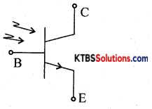
What is a phototransistor? Draw its symbol,
Answer:
The phototransistor is a light-sensitive device,
Symbol:
PART-C
Answer any FIVE of the following questions. (5 × 3 = 15)
Question 19.
Mention a few applications of the internet.
Answer:
The Internet provides several applications like World wide web, e-mail, e-commerce, chat, teleconference, and telemedicine.
Question 20.
Define the following terms with respect to an AC signal.
(a) Cycle
Answer:
Cycle: AC frequency is the number of cycles per second in an alternating current (ac)
(b) frequency
Answer:
Frequency: The frequency of ac is the number of cycles per second.
(c) Time period
Answer:
Time period: Time period is the time taken by ac for one complete cycle.
![]()
Question 21.
Explain the construction of a carbon composition resistor.
Answer:
A mixture of finely divided carbon and a powdered insulating material forms the resistor element. The mixture is more Ided into a cylindrical shape. The proportion of the mixture is adjusted to get the desired value of resistance. Metal caps with leads of tinned copper wire are joined to two ends of a carbon-coated resistor for external connection. As the leads are joined axially from the ends, they are called axial leads. The non-conductive material is coated on the resistor element for insulation and mechanical strength. To specify the resistance of the resistor, a band of colors is marked on the body of the resistor.
Carbon composition resistors are smaller in size and cheap. They are available in the resistance range of 1Ω to 20MΩ. Their power rating is \(\frac{1}{10}, \frac{1}{8}, \frac{1}{4}, \frac{1}{2}\)1 and 2W. These resistors are used where accuracy is not important.
Question 22.
A step-down transformer is used to reduce the main supply of 220 V to 10 V. If the primary draws 5A and secondary 100 A. Calculate the efficiency of the transformer.
Answer:
P =Vp × I = 220 × 5 = 1100W
P =V × I = 10 × 100 = 1000W
η = \(\frac{P_{\text {out }}}{P_{\text {in }}}\) × 100 = 91%
Question 23.
Explain with a circuit diagram and graph the growth of current in an RL network.
Answer:
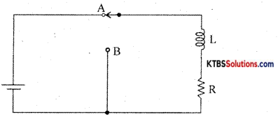
Consider an inductor Land a resistor R connected in series to a cell. When the switch is in position A, the current in the circuit grows exponentially.
The current 1 at a time after the switch is placed in position A is I = I0e-(R/L)t, where I0 is the maximum current.
The time constant of RL circuits is the time taken by the current to grow to 63.2% of the maximum value.
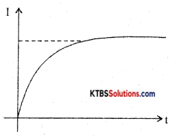
Growth of current in RL circuit
![]()
Question 24.
Derive an expression for the resonant frequency of a series resonant circuit.
Answer:
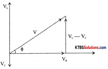
Consider an AC circuit consisting of inductance (L), capacitor C and a resistance R connected in series to an AC source. Let the instantaneous voltage of the ac source be
v = Vm sin wt
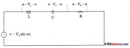
Let VL, VR, Vc be the voltages across the inductor, Resistor, and capacitor.
Question 25.
Classify solids based on the energy band diagram.
Answer:
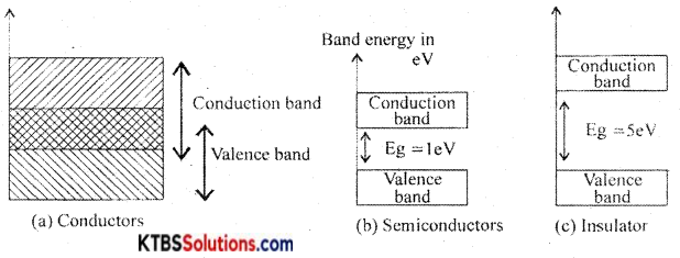
Conductors: These are materials that allow the current to flow through them easily. In conductors, the valence band and conduction band overlap completely due to which the valence electrons drift to the conduction band easily. Even at room temperature, there is a large number of free electrons. Hence due to the small voltage applied a large current flows through them.
Semiconductors: These are the materials with electrical conductivity lying between those of conductors and insulators. The forbidden energy gap between the valence band and conduction band is 0.7 eV for germanium and I. I eV for silicon. At absolute zero, a semiconductor acts as an insulator. As the temperature increases, more valence electrons jump to the conduction band. Hence the conductivity of semiconductors increases with an increase in their temperature.
Insulators: insulators are materials that do not allow the electric current to flow through them easily. The valence band is completely filled and the conduction band is completely empty in insulators. The forbidden energy band between the conduction band and valence band is nearly 5eV. In the conduction band, there are no free electrons present at room temperature. Hence, the insulators do not conduct at all at room temperature.
![]()
Question 26.
Write the steps involved in PCB designing.
Answer:
- PCB layout preparation.
- photo-resist.
- PCB etching process
- PCB drilling.
- Conductor plating.
- PCB Assembling
PART-D
I. Answer any THREE of the following questions:
Question 27.
Find the branch currents in fig. below.
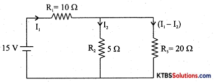
Answer:
10 I1 + 5 I2 = 15 ….(1)
20(I1 – I2) – 5I2 = 0
20(I1 – 25I2) = 0 ….(2)
Solving I1 = 1.07 A
I2 = 0.856 A
I1 – I2 = 0.21 A
Question 28.
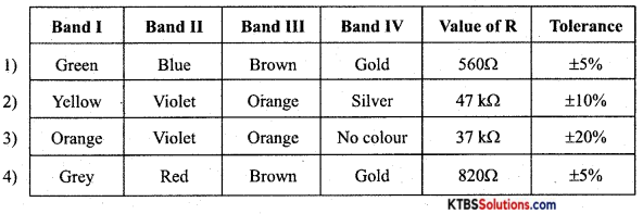
Complete the following table for the carbon resistor R.
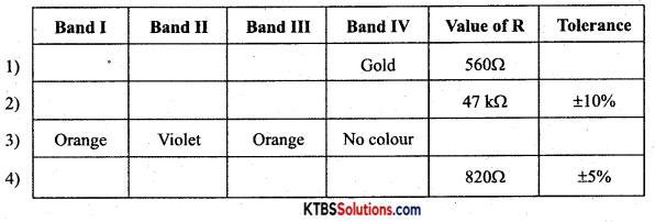
Answer:
Question 29.
An inductor of 20 mH is connected in series with a resistor of 50W. The combination is connected to 220V, 50 Hz, source. Find the current in the circuit.
Answer:
XL = 2πfL = 6280 × 10-3H = 6.28H .
Z = \(\sqrt{\mathrm{R}^{2}+\mathrm{X}_{\mathrm{L}}^{2}}\) = 50.39Ω
I = \(\frac{Y}{Z}=\frac{220}{50.39}\) = 4.36 A
Question 30.
In the circuit shown below find the value of series resistance Rs if Zener current is 10 mA.
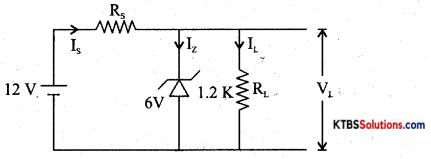
Given: Vs = 12 V, Vz = 6, RL = 1.2 KΩ
Answer:
VL = Vz = 6V
IL = \(\frac{\mathrm{X}_{\mathrm{L}}}{\mathrm{R}_{\mathrm{L}}}\) = 5mA
Iz = 10 m A
Is = Iz + IL = 15mA
Rs = \(\frac{V_{S}-V_{Z}}{I_{S}}\) = 4ooΩ
Question 31.
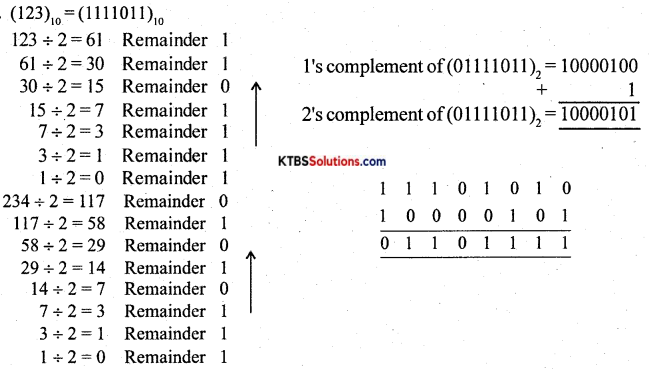
Subtract (123) from (234) using 2’s complement method.
Answer:
PART-E
Answer any FOUR questions. (4 × 5 = 20)
Question 32.
State and explain the superposition theorem with an example.
Answer:
In any linear bilateral network consisting of two or more independent sources, the resultant current or voltage in any branch ¡s the algebraic sum of the currents or voltages caused by each independent source acting alone, with all other independent sources being replaced by their internal resistances.
Procedure for using Superposition Theorem:
Step 1: Retain the source V1 and replace all other sources with their internal resistances.
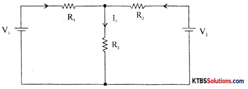
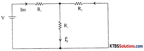
Step 2: Current in various branches and their voltage drops due to V1 alone are determined as follows,
RT1 = R1 + \(\frac{\mathrm{R}_{2} \mathrm{R}_{3}}{\mathrm{R}_{2}+\mathrm{R}_{3}}\)
Im1 = \(\frac{\mathrm{V}_{1}}{\mathrm{R}_{\mathrm{T}_{1}}}\)
I’3 = Im1 × \(\frac{R_{2}}{R_{2}+R_{3}}\) {from branch current formula}
Voltage across R3 = V’3 = I’3 = I”1 = Im2 × \(\frac{R_{1}}{R_{1}+R_{3}}\)
Step 3 : Consider V2 alone and find the currents and voltages as follows:
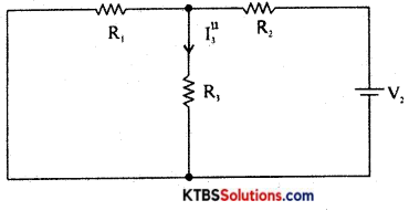
RT2 = R2 + \(\frac{\mathrm{R}_{1} \mathrm{R}_{3}}{\mathrm{R}_{1}+\mathrm{R}_{3}}\)
Im2 = \(\frac{\mathrm{V}_{2}}{\mathrm{R}_{\mathrm{T}_{2}}}\)
I”3 = V2 × \(\frac{\mathrm{R}_{1}}{\mathrm{R}_{1}+\mathrm{R}_{3}}\)
Step 4: Find the algebraic sum of currents and voltage drops in a branch.
I3 = I’3 + I”3; V’3 = I’3R3, V = I”3R3
V3 = V’3 + V”3
Question 33.
(a) Derive an expression for the equivalent capacitance of two capacitors connected in series.
Answer:
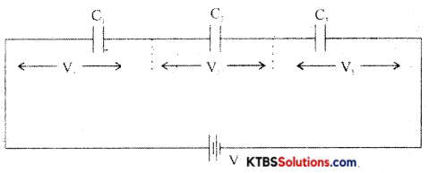
In a series combination, the capacitors are connected end to end. The charge on each capacitor is the same and the emf of the cell equals the sum of voltages across the three resistors.
Consider three capacitors C1, C2, C3 connected in series.
Then V = V1 + V2 + V3
= \(\frac{\mathrm{Q}}{\mathrm{C}_{1}}+\frac{\mathrm{Q}_{1}}{\mathrm{C}_{2}}+\frac{\mathrm{Q}}{\mathrm{C}_{3}}\)
V = Q\(\left(\frac{1}{C_{1}}+\frac{1}{C_{2}}+\frac{1}{C_{3}}\right)\) …………(1)
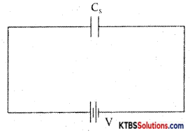
Let the combination be replaced by an equivalent capacitor Cs which has the same effect as the combinations of capacitors. If Cs is the effective capacitance.
then v = \(\frac{\mathrm{Q}}{\mathrm{C}_{\mathrm{s}}}\) →(2)
From equn (1) and (2)

The reciprocal of the effective capacitance of capacitors in series is the sum of reciprocals of individual capacitances.
(b) What are the functions of capacitors.
Answer:
Capacitors are used.
- to store charges.
- in power supplies.
- in avoiding sparking.
- to provide different voltages.
![]()
Question 34.
Draw and explain the V-I characteristic of a P-N junction diode.
Answer:
The V-I characteristic of a diode is the graph between the voltage across the diode and the current flowing through it.
The V-I characteristics can be divided into two parts namely
- Forward characteristics
- Reverse characteristics.
1. Forward characteristics of semiconductor diode:
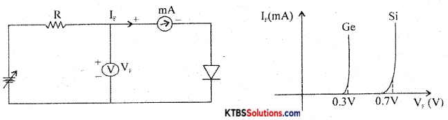
The circuit for plotting V-I characteristics of the diode is as shown. The resistance R limits the current to a permissible value. A voltmeter measures the voltage across the diode and the milliammeter reads the current flowing through the diode.
The forward voltage VF is increased in steps of 0.1 V and the corresponding forward current VF is noted. A graph of VF along the x-axis and corresponding VF along the y-axis gives the forward characteristics curve.
Diode current is zero when VF 0. When VF is more than barrier potential, current VF increases. The forward voltage VF at which forward current starts to increase rapidly is called the knee voltage or cut-in voltage or threshold voltage (VK). For germanium diode, VK 0.3 V and for silicon diode, VK = 0.7V.
Reverse characteristics of a pn junction:
The circuit for plotting reverse characteristics of a diode is shown below
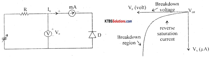
The reverse voltage is increased gradually till the diode starts conducting and the corresponding reverse currents are noted. On platting a graph between reverse voltage and reverse current, the characteristic curve is as shown.
Due to reverse bias applied on pn junction, an extremely small current ‘R (few μA) flows through the diode. The reverse current remains almost constant up to the breakdown voltage. After this point, for a small change in reverse voltage, the reverse current increases very rapidly. This sudden flow of large current may destroy the diode due to overheating. Hence, the diode should be operated in the reverse bias with reverse voltage less than break down voltage.
Question 35.
What is a filter circuit?
A circuit diagram explains the working of a shunt capacitor filter. Draw the input and output waveforms.
Answer:
Question 36.
(a) Simplify the Boolean equation Y = ABC + AB̅C + A̅BC̅ and draw the logic diagram.
(b) State and prove De-Morgan’s theorem.
Answer:
Y = ABC + AB̅C + A̅BC̅
= AC(B + B̅) + A̅BC̅
= AC. 1 + A̅BC̅ {∵ B + B̅ = 1}
= AC + A̅BC̅
Question 37.
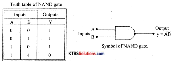
Explain with the DTL circuit the action of a two-input NAND gate.
Answer:
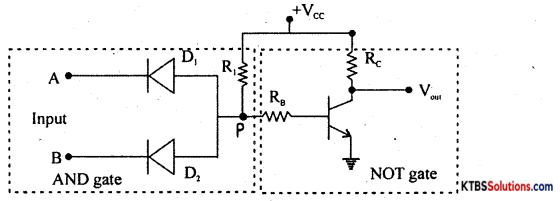
Case (i) When both inputs A and B are LOW (0V), both the diodes D1 and D2 are forward biased. Hence voltage at junction P of the diode becomes zero. This makes the transistor Q go to cut off. Hence the output at the collector of the transistor becomes HIGH.
Case (ii) When A is LOW and B is HIGH, D is forward biased and D2 is reverse biased. Hence the voltage at P becomes zero. This makes the transistor go to a cut-off state and therefore output at its collector becomes HIGH.
Case (iii) When A is HIGH and B is LOW, D1 is reverse biased and D2 is forward biased due to which voltage at P is zero. This makes the transistor go to a cut-off state and therefore output at its collector becomes HIGH.
Case (iv) When both the inputs are HIGH, D1 and D2 are reverse biased. Hence voltage at P becomes +V. This makes the transistor Q go to saturation and the transistor acts like a closed switch. Therefore output becomes LOW.