Students can Download 1st PUC Electronics Previous Year Question Paper March 2020 (North), Karnataka 1st PUC Electronics Model Question Papers with Answers helps you to revise the complete syllabus.
Karnataka 1st PUC Electronics Previous Year Question Paper March 2020 (North)
Time: 3.15 Hours
Max Marks: 70
Instructions:
- The question paper contains four parts.
- Part – A is compulsory,
- Part – D contains two subparts (i) Problems and (ii) Essay type questions.
- Draw circuit diagrams wherever necessary
PART-A
Answer ALL the following questions: (10 × 1 = 10)
Question 1.
Expand JEET.
Answer:
Junction Field Effect Transistor.
Question 2.
Define node in a circuit.
Answer:
Node is a point in a circuit where the current divides.
Question 3.
Write the symbol of the Ohm meter.
Answer:
![]()
Question 4.
Name a passive component that is used to limit the flow of current in DC circuits.
Answer:
Resistor.
![]()
Question 5.
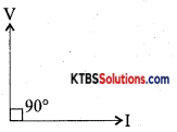
Draw the phasor diagram of voltage and current in a purely inductive circuit.
Answer:
Question 6.
What is the forbidden energy gap of a silicon semiconductor?
Answer:
The forbidden energy gap is the separation between the conduction band and valence band in the energy band diagram. Its value is 1 eV in the case of silicon semiconductors.
Question 7.
Draw the symbol of a varactor diode.
Answer:
![]()
Question 8.
Which is the heavily doped region of a transistor?
Answer:
Emitter.
Question 9.
To which number system DB6 belong?
Answer:
Hexadecimal number system.
Question 10.
Mention any one type of seven-segment display.
Answer:
Common anode seven segment display.
PART-B
Answer any FIVE of the following questions. (5 × 2 = 10)
Question 11.
Give two examples for semiconductor devices.
Answer:
Glucometer, Pulse oximeter.
Question 12.
What are active and passive components? Give one example for each.
Answer:
Active components supply energy to a circuit, and they can process a signal.
E.g.: Diode, Transistor, FET, SCR.
Passive components absorb energy and cannot supply energy.
E.g.: Resistor, Capacitor, Inductor.
Question 13.
Mention any four controls of a multimeter.
Answer:
Range switch, DC voltage range switch, AC voltage range switch, ohm range switch, current range switch.
Question 14.
Define inductive reactance. Mention its unit.
Ans.
Inductive reactance is the opposition offered to the flow of ac by the inductor. Its unit is henry.
![]()
Question 15.
Write any two applications of LED.
Answer:
- LED is used as a power indicator.
- LED is used in optical fiber communication.
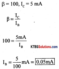
Question 16.
An npn transistor has a DC current gain of 100. Calculate the base current when the collector current is 5 mA.
Answer:
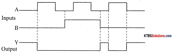
Question 17.
Sketch the timing diagram of a NOR gate.
Answer:
Question 18.
What is etching?
Answer:
Etching is the process of removing unnecessary copper by exposing it to ultraviolet rays.
PART-C
Answer any FIVE of the following questions. (5 × 3 = 15)
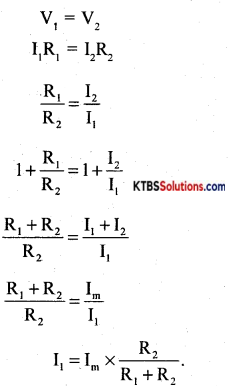
Question 19.
Explain the current divider rule.
Answer:
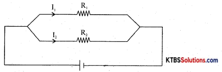
As resistors are in parallel,
Question 20.
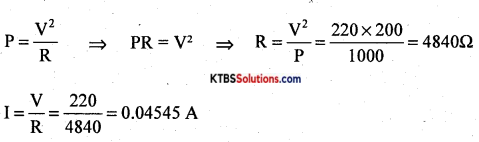
The specification of an ¡ron box is labeled as 220V, 1000 W. What is its resistance? Also, find the current through it.
Answer:
V= 220V, P = 1000W
![]()
Question 21.
Explain the principle of the capacitor.
Answer:
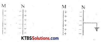
Consider two metal plates M and N separated by a small distance. Let the inner surface of metal plate M be positively charged. Then due to electrostatic induction, an equal and opposite negative, the charge is induced on the inner surface of metal plate N and an equal positive charge is induced on the outer surface of plate N.
The negative charge on N tries to decrease the potential on M and the positive charge on N tries to increase the potential on M. As the negative charges on plate N are nearer to plate M, it has a greater effect on plate N. Hence, there is a net decrease in potential on M and thus the capacitance of the capacitor increases. If the outer surface of plate N is grounded (or connected to earth), the charges on the outer surface of plate N are neutralized.
Due to negative charges only on plate N, the potential of plate M is greatly reduced. Hence the capacitance of plate M increases. When the grounded conductor is placed near a charged conductor with a dielectric medium in between, the capacitance of the system increases.
The capacitance of the capacitor can be increased by
- reducing the distance between the plates.
- placing the medium of a high dielectric constant between the plates of the capacitor.
Question 22.
Classify the solids based on the energy band diagram.
Answer:
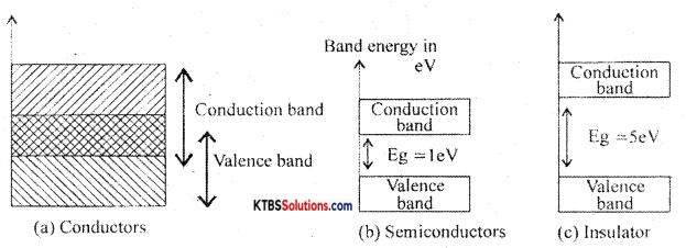
Conductors: These are materials that allow the current to flow through them easily. In conductors, the valence band and conduction band overlap completely due to which the valence electrons drift to the conduction band easily. Even at room temperature, there is a large number of free electrons. Hence due to the small voltage applied a large current flows through them.
Semiconductors: These are the materials with electrical conductivity lying between those of conductors and insulators. The forbidden energy gap between the valence band and conduction band is 0.7 eV for germanium and 1. 1 eV for silicon. At absolute zero, a semiconductor acts as an insulator. As the temperature increases, more valence electrons jump to the conduction band. Hence the conductivity of semiconductors increases with an increase in their temperature.
Insulators: Insulators are materials that do not allow the electric current to flow through them easily. The valence band is completely filled and the conduction band is completely empty in insulators. The forbidden energy band between the conduction band and valence band ¡s nearly 5eV. In the conduction band, there are no free electrons present at room temperature. Hence, the insulators do not conduct at all at room temperature.
![]()
Question 23.
Draw and explain the forward V-I characteristics of a semiconductor diode.
Answer:
The V-I characteristics of a diode are the graph between the voltage across the diode and the current owing through it.
The V-I characteristics can be divided into two parts namely
- Forward characteristics
- Reverse characteristics.
1. Forward characteristics of semiconductor diode:
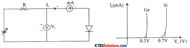
The circuit for plotting V-I characteristics of the diode is as shown. the resistance R limits the current to a permissible value. A voltmeter measures the voltage across the diode and the milliammeter reads the current flowing through the diode.
The forward voltage VF is increased in steps of 0.1 V and the corresponding forward current VF is noted. A graph of VF along the x-axis and corresponding VF along the y-axis gives the forward characteristics curve.
Diode current VF is zero when VF = 0. When VF is more than barrier potential, current VF increases. The forward voltage VF at which forward current starts to increase rapidly is called the knee voltage or cut-in voltage or threshold voltage (VK). For germanium diode, VK = 0.3 V and for silicon diode, VK = 0.7V.
Reverse characteristics of a p-n junction:
The circuit for plotting reverse characteristics of a diode is shown below
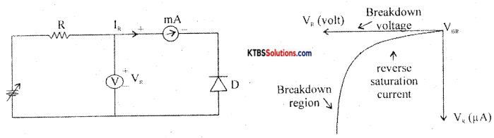
The reverse voltage is increased gradually till the diode starts conducting and the corresponding reverse currents are noted. On platting a graph between reverse voltage and reverse current, the characteristic curve is as showñ.
Due to reverse bias applied on the p-n junction, an extremely small current IR (few μA) flows through the diode. The reverse current remains almost constant up to the breakdown voltage.
After this point, for a small change in reverse voltage, the reverse current increases very rapidly. This sudden flow of large current mA destroys the diode due to overheating. Hence, the diode should be operated in the reverse bias with reverse voltage less than break down voltage.
Question 24.
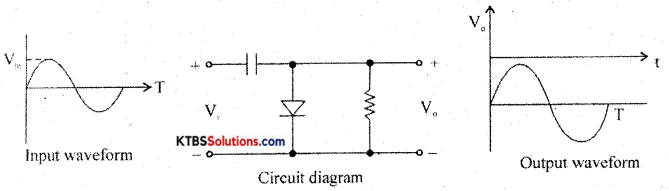
Explain the working of a positive diode clamper with input and output waveforms.
Answer:
A negative clamper is a circuit that clamps the negative peak of a signal to a desired de level.
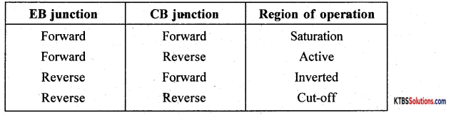
Question 25.
Mention the different ways of biasing the base-emitter and collector-base junctions of a transistor and their respective regions of operatIon.
Answer:
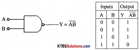
Question 26.
A logic gate produces a HIGH output when any one of its inputs is LOW and produces a LOW output when the alt of its inputs are HIGH. Identify the gate. Draw its logical symbol and truth table.
Answer:
PART-D
I. Answer any three of the following questions: (3 × 5 = 15)
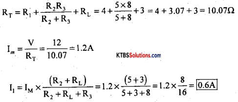
Question 27.
Calculate the circuit through 8Ω using the branch current method.
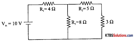
Answer:
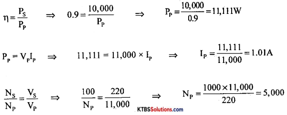
Question 28.
A step-down transformer of90% efficiency and power output of 10kW reduces the voltage from 11kV to 220V. Calculate
(i) number of turns in the primary if the number of turns in 4he secondary is 100
(ii) current in the primary.
Answer:
Ps = 10kW = 10,000W
Vp = 11,000V, Vs = 200V, Ns = 100
![]()
Question 29.
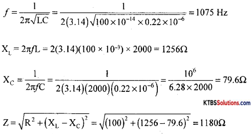
Calculate the resonant frequency and impedance of a series LCR circuit with R = 100Ω, C = 0.22 μF, and L = 100 mH are connected to an ac signal of 230V 2000 Hz.
Answer:
Question 30.
In a voltage regulator circuit shown, calculate
(i)Load voltage
(ii) Current through R
(ii) Current through R1
(iv) Current through the Zener
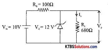
Answer:
VL = Vz = 12V.
Vs = VB – Vz = 20 – 12 = 8v
IL = \(\frac{\mathrm{V}_{\mathrm{L}}}{\mathrm{R}_{\mathrm{L}}}=\frac{12}{680}\) =17.6rnA
Is = \(\frac{V_{S}}{R_{S}}=\frac{8}{100}\) =80mA
Iz = Is – IL = 80 – 17.6 = 62.4mA
Rs = \(\frac{\mathrm{V}_{\mathrm{S}}-\mathrm{V}_{\mathrm{Z}}}{\mathrm{I}_{\mathrm{S}}}\) = 400Ω
Question 31.
Perform the following operations
(i) (11011)2 ÷ (100)2
Answer:
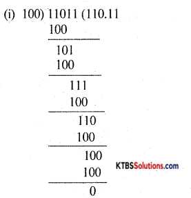
11011 100 = (110.11)
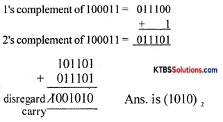
(ii) (101101)2 – (100011)2 using 2’s complement method (2 + 3)
Answer:
PART-E
Answer any FOUR questions. (4 × 5 = 20)
Question 32.
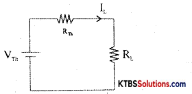
State Thevenin’s theorem with necessary circuit diagrams, explain how to Thevenise a circuit.
Ans.
Thevenin’s theorem states that any linear bilateral network having several voltage sources and resistors can be replaced by a simple circuit having one voltage source V in series with one single resistor RTh.”
Step 1: Identify and remove load resistor RL to convert the circuit as a two-terminal network. Mark the two terminals as A and B.
Step 2: To find VTh, calculate the open-circuit voltage between terminals A and B.
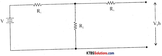
VTh = VR2 = \(\frac{V}{R_{1}+R_{2}}\) × R2
Step 3: To find R, replace all voltage sources in the network with their internal resistances and then find the effective resistance between terminals A and B.
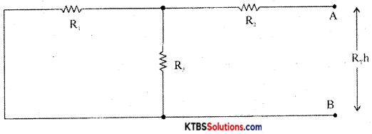
Step 4: Construct Thevenin’s equivalent circuit having V in series with R and reconnect the load resistor which was earlier removed.
IL = \(\frac{\mathrm{V}_{\mathrm{Th}}}{\mathrm{R}_{\mathrm{Th}}+\mathrm{R}_{\mathrm{L}}}\)
VL = ILRL.
![]()
Question 33.
With necessary circuit diagrams, derive the expression for the effective capacitance of two capacitors connected in series.
Answer:
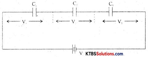
In a series combination, the capacitors are connected end to end. The charge on each capacitor is the same and the emf of the cell equals the sum of voltages across the three resistors.
Consider three capacitors C1, C2, C3 connected in series.
Then V = V1 + V2 + V3.
= \(\frac{\mathrm{Q}}{\mathrm{C}_{1}}+\frac{\mathrm{Q}_{1}}{\mathrm{C}_{2}}+\frac{\mathrm{Q}}{\mathrm{C}_{3}}\)
V = Q\(\left(\frac{1}{C_{1}}+\frac{1}{C_{2}}+\frac{1}{C_{3}}\right)\) ……….(1)
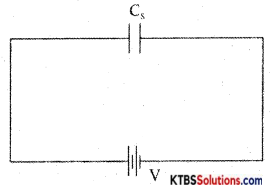
Let the combination be replaced by an equivalent capacitor Cs which has the same effect as the combinations of capacitors. If Cs is the effective capacitance.
then V = \(\frac{\mathrm{Q}}{\mathrm{C}_{\mathrm{s}}}\) → (2)
From equn (1) and (2)
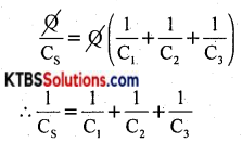
The reciprocal of the effective capacitance of capacitors ¡n series is the sum of reciprocals of individual capacitances.
Question 34.
Describe the construction and working of a loudspeaker.
Answer:
A loudspeaker is a transducer that changes electrical energy into sound waves of varying pressure.
- a coil of wire called a voice coil.
- a permanent magnet
- a cone-shaped piece of stiff paper or cloth called the diaphragm.
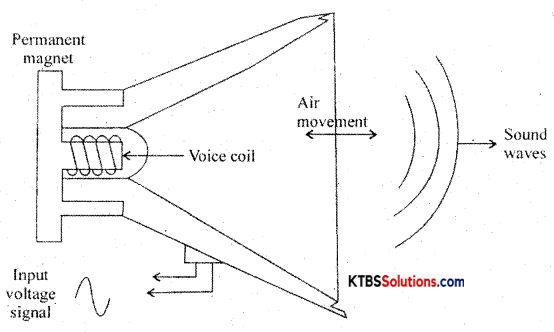
Voice coil is suspended in the strong magnetic field of a circular permanent magnet. The permanent magnet of a speaker provides a steady magnetic field. The two leads of the voice coil are connected with wire to terminals on the speaker frame.
When audio signal current flows through the voice coil, it produces varying magnetic fields in the coil. The varying magnetic field moves the voice coil in and out in accordance with variations in the electrical audio signals. Hence the diaphragm attached to the voice coil vibrates due to which compressions and rarefactions are formed and the sound waves are produced.
Question 35.
(a) With a neat diagram and graph, explain the growth of current in an RL circuit
Answer:
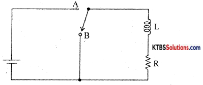
When the switch is in position A, the current in the circuit increases exponentially and reaches a maximum value. When the switch is in position B, the current in the circuit starts decaying exponentially with time.
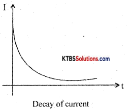
The value of current at target after the switch is placed in position B is I = I0e(-R/L)t where I0 is the maximum current.
The time constant of the RL circuit is the time taken by the RL circuit for the current to decay to 36.8% of its maximum value.
(b) Determine the time constant of a RL circuit having R = 100Ω and L = 100 mil. (3+ 2)
Answer:
T = \(\frac{\mathrm{L}}{\mathrm{R}}=\frac{100 \times 10^{-3}}{100}\) = 1ms
![]()
Question 36.
With a neat diagram, explain the working of a half-wave rectifier. Draw the input and output waveforms.
Ans.
Half wave rectifier is a circuit that removes one-half cycle of the AC input and produces a pulsating DC output voltage.
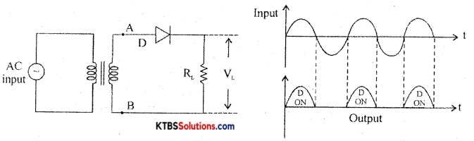
It has diode D ¡n series with a load resistor RL. The AC mains voltage to be rectified is applied to the primary of a transformer and voltage induced across secondary is applied to the rectifier.
During the positive half cycle, A is positive and B is negative. The diode ¡s forward biased and conducts and the diode acts as a closed switch. Hence, the positive half cycle of the voltage is developed across the load resistor RL.
During a negative half cycle, A is negative and B is positive. The diode is reverse biased and does not conduct as it acts as an open switch. Hence there ¡s no output. The output waveform across RL has only positive half cycles. Ripple factor is the ratio of the RMS value of(r) the AC component of the load voltage to the average value of load voltage.
r = \(\frac{\text { rms value of AC component }}{\text { value of dc component }}\) = 1.21
Rectifier efficiency is the ratio of de output power to ac input power.
η = \(\frac{\text { DC output power }}{\text { AC input power }}\) = 0.406 or 40.6%
Question 37.
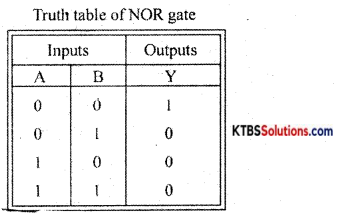
Explain the working of a DTL NOR gate.
Answer:
NOR gate is a logic circuit whose output is HIGH only when both its inputs are LOW
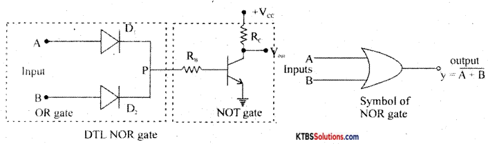
Diodes D1 and D2 form OR gates and the transistor act as NOT gate.
Case (i) When A = 0, B = 0, the diodes are not forward biased and they do not conduct. Hence voltage P is zero. This zero voltage makes the transistor go to cut-off condition and therefore output is HIGH.
Case (ii) When A = 0, B = 1, D1 does not conduct but D2 conducts. Hence voltage at P is +Vcc and it drives the transistor to saturation and output becomes LOW.
Case (iii) When A = 1, B = O, D1 conducts and D2 does not conduct. Hence voltage at P is +Vcc and this makes the transistor Q go to saturation. Hence output becomes LOW.
Case (iv) When A = 1, B = 1, both diodes conduct as they are forward biased. Then voltage at P is +Vcc and the transistor is driven to saturation. The output at the collector becomes LOW.