Students can Download 2nd PUC Electronics Model Question Paper 1 with Answers, Karnataka 2nd PUC Electronics Model Question Papers with Answers helps you to revise the complete Karnataka State Board Syllabus and score more marks in your examinations.
Karnataka 2nd PUC Electronics Model Question Paper 1 with Answers
Max Marks: 70
Time : 3 hrs. 15min.
Part – A
Answer all questions: 10 x 1 = 10
Question 1.
Expand the term FET.
Answer:
FET = Field Effect Transistor.
Question 2.
Which region of a transistor acts as a closed switch?.
Answer:
Saturation Region
Question 3.
Mention one application of a comparator.
Answer:
Zero crossing detector or Schmitt Trigger.
![]()
Question 4.
What is over modulation in AM?
Answer:
If modulation index is greater than 1, then it is called over modulation in AM.
Question 5.
Mention the frequency range of FM super heterodyne receiver.
Answer:
88 to 108 MHz.
Question 6.
Name the power device used in controlled rectifier?
Answer:
Power diode
Question 7.
Write the BCD code for (23)10.
Answer:
(23)10 = (0010 0011)2
Question 8.
Which code is used in shaft position encoders?
Answer:
Gray code.
Question 9.
How many register banks are present in 8051?
Answer:
4
![]()
Question 10.
What is the command to execute a program in UNIX system?
Answer:
sh.
Part-B
Answer any Five questions. 5 x 2 = 10
Question 11.
Name two types of JFET.
Answer:
- n channel FET
- p channel FET
Question 12.
Mention any two characteristics of a CC amplifier.
Answer:
High input impedance and low output impedance.
Question 13.
Mention the different types of negative feedback.
Answer:
- Voltage shunt feedback
- Voltage series feedback
- Current series feedback
- Current shunt feedback
![]()
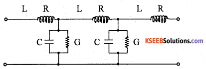
Question 14.
Draw the equivalent circuit of transmission lines for low frequency.
Answer:
Question 15.
Give the reason for the presence of drift layer in a power diode.
Answer:
The drift layer decreases the resistivity of the power diode under forward biased condition.
Question 16.
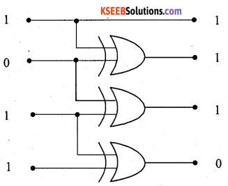
Convert (1011)2 into gray code using XOR gates
Answer:
Question 17.
Mention any two types of errors that occur in C programming.
Answer:
Syntax, errors, Logical errors, Run time errors.
Question 18.
Explain what is meant by cell splitting.
Answer:
Cell splitting is dividing entire geographical area into hexadecimal shaped cells that fit together to form honey comb pattern.
Part – C
Answer any Five questions. 5 x 3 = 15
Question 19.
Derive the equations to determine the coordinates of Q point in voltage divider bias.
Answer:
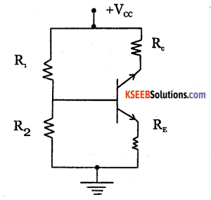
Voltage across R2 is
\(\mathrm{V}_{2}=\frac{\mathrm{V}_{C C} \mathrm{R}_{2}}{\mathrm{R}_{1}+\mathrm{R}_{2}}\)
Applying KVL to the base circuit , We get
V2 = VBE + V2
V2 = VBE + IE RE
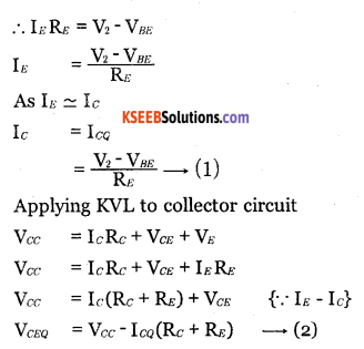
Equations 1 and 2 define operating point or Q point.
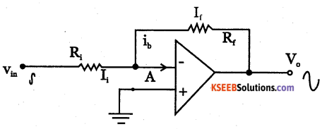
Question 20.
With a block diagram derive an expression of output impedance of negative feedback amplifier.
Answer:
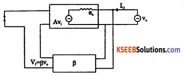
An amplifier should have a low output impedance so that it can deliver power to load without much loss. With negative feedback, the output impedance of the amplifier decreases which is desirable.
Let Zo be output impedance of basic amplifier and Zof be the output impedance with negative feedback. A hypothetical source of voltage Vo is applied at the output. By applying KVL to the output loop,
Vo = IoZo +AVi.
With negative feedback, input to basic amplifier with negative feedback is
Vi = Vs – Vf
Vi = o – Vf
Vi – Vf
{As input is short circuited, V = o}
As 1+Aβ>1,output impedance of amplifier decreases by a factor(1+Aβ)
![]()
Question 21.
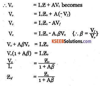
With a circuit diagram explain the working of Wien bridge oscillator.
Answer:
The circuit diagram shows wein bridge oscillator in which wein bridge is connected between amplifier input terminal and the output terminal. The bridge has a series RjC, network in one arm and a parallel R2C, network in the adjoining arm. In the remaining arm of the bridge, resistors R3, R4 are connected. The phase angle criterion for oscillation is that total phase shift around the circuit should be 0°.
This is possible only when output is fedback to the noninverting input without any phase shift since the lead-lag network does not produce any phase shift. This condition occurs only when the bridge is balance i.e., at resonance. The frequency of oscillation is given by \(f=\frac{1}{2 \pi R C}=\frac{0.159}{R C}\)
The feedback fraction, β = \(\frac{1}{3}\)
Question 22.
Mention the different layers of Ionosphere and explain each layer.
Answer:
Ultraviolet radiation from the sun cause the upper atmosphere to ionize i.e. to become electrically charged. Hence a thick layer of ions formed at heights of 50 km to 400km. The ionosphere supports MF and HF wave propagation.
Its three layers are:
D layer: It is at a height of 70 km and has an average thickness of 10 km. It disappears in the night time. It reflects VLF and LF waves and absorbs MF and HF waves.
E layer: It is at a height of 100 km with a thickness of 25 km. This layer disappears at night. It helps in MF and HF wave propagation.
F layer: It is at a height of 150 km and extends upto 400 km. This layer exists during both day and night time. During day time, it splits into two layers F, and F2, and combines to form a single F layer during night time.
| F2 region. 250-400 km. |
| F1 region. 160-250 km. |
| E region. 95-130 km |
| D region. 50-95 km. |
| Troposphere Earth. |
![]()
Question 23.
Draw the circuit diagram of single phase AC voltage controllers with input and output waveforms.
Answer:
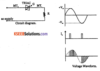
TRIAC is a bi-directional solid state device and conducts in both halves of ac supply. During positive half cycle MT2 becomes positive wrt MT, and gate becomes positive wrt MTr TRIAC conducts when gate pulse is injected at a firing angle a. The current follows TRIAC in the voltage wave shape from angle α to π At π, the zero crossing of the supply voltage, the TRIAC is switched OFF due to line commutation.
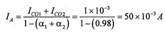
Question 24.
Determine anode current IA of SCR when Ic = 0. Given (α1 + α2) = 0.98 and
(1C01 + 1C02) = 1mA.
Answer:
Question 25.
Write an assembly language program to add 05H and OAH and store the result in R2.
Answer:
MOV A, #05H ; load 05H into A.
ADD A,# OAH ; add OA to 05H.
MOVR2,A ; A = A + 05H.
NOP; load A to R5
END.
Question 26.
Mention few application of satellites.
Answer:
- Voice communication.
- TV and radio broadcast.
- Teleconferencing.
- Mobile communication.
Part – D
Answer any Three questions: 3 x 5 = 15
Question 27.
Calculate the voltage gain, input impedance and output impedance in the circuit given below. Given β = 100 and \(r_{ e }=\frac { 26mv }{ { I }_{ { E } } } \)
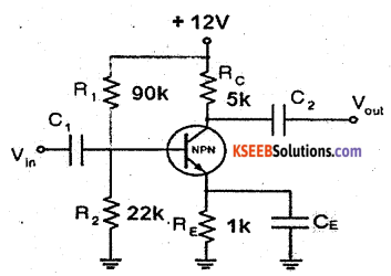
Answer:
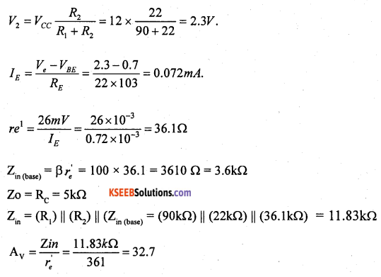
![]()
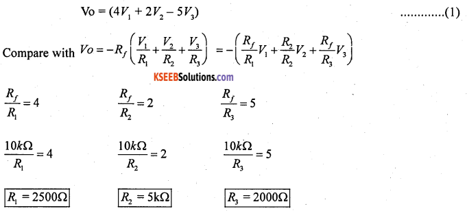
Question 28.
Design an adder using an op-amp to get the output expression as
Vo = (4V1+ 2V2 – 5V3) where Rf = 10 kΩ.
Answer:
Question 29.
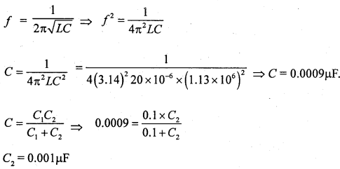
A colpitts oscillator oscillates at 1.13MHz. If the inductor in the feedback network has a value of 20pH and one of the capacitor values is 0.1pF, calculate the value of the other capacitor.
Answer:
f= 1.13 MHz = 1.13 x 10⁶ Hz
L = 20 μH = 20 x 10-6 H
C1 = 0.1 μH = 0.1 x 10⁻⁶ H
Question 30.
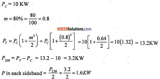
A 10 kW carrier wave is amplitude modulated at 80% depth of modulation by a sinusoidal modulating signal. Calculate the total power and sideband power of the AM wave.
Answer:
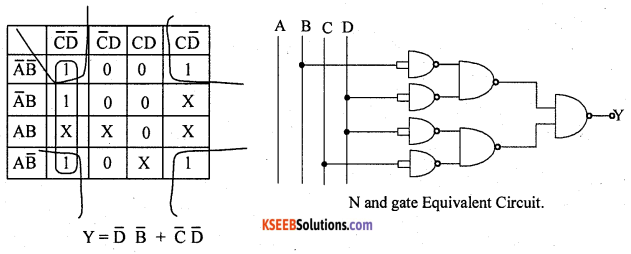
Question 31.
Simplify the Boolean expression Y=Σm (0,2, 4,8,10) + ∑d (11,12,13,14) using K- map. Draw the NAND Gate equivalent circuit to realize the simplified equation.
Answer:
Part – E
Answer any Four questions. 4 x 5 = 20
Question 32.
With a circuit diagram explain the working of class B push pull amplifier.
Answer:
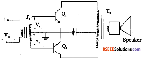
Class B push-pull amplifier is as shown in the diagram. T1 and T2 are two centre tapped transformers and Q1, Q2 are two identical transistors. Transformer T1 produces signal voltages V1 and V2 which are 180° out of phase with each other.
These two signals are applied to the Polarities reverse during negative half cycle of input voltage. Q2then is ON and Q1 is OFF. Q2amplifies the signal and the alternate half cycle appears across the loud speaker.
![]()
two transistors. Transformer T2 couples AC output signal from collector to loud speaker. The two emitters are connected to centre tap of transformer T1 secondary and Vcc to the centre tap of T2 secondary.
During positive half cycle of input voltage, secondary winding of T1 has voltages V, and V2. Transistor Q1, conducts and Q2 is cut off. The collector current through Q1 produces an amplified and inverted voltage which applied to loud speaker through a transformer.
Question 33.
(a) Explain how an operational amplifier can be uses as an integrator?(1 + 4)
Answer:
Integrator is a circuit whose output is proportional to integral of its input.
(b) Mention any four characteristic of ideal OP – Amp.
Answer:
| Characteristics | Ideal op amp | Practical op – amp |
| open loop gain | ∞ | 105 |
| Input impedance | ∞ | Few M Q. |
| Output impedance | 0 | Few ohm. |
| Bandwidth | ∞ | Few MHz. |
| CMRR | ∞ | 90 dB |
Question 34.
Draw the block diagram of AM SHD receiver and explain the function of each block.
Answer:
RF amplifier: The RF amplifier increases the signal strength before the signal is fed to mixer
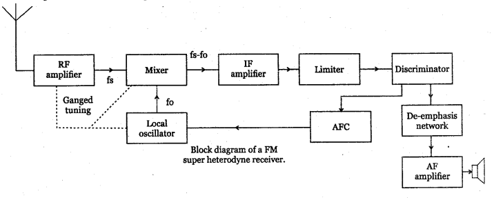
when turned to the desired frequency. The RF amplifier is designed to handle large bandwidth of 150 kHz.
Mixer: the incoming RF signal of frequency fm is applied to a mixer which also receives the output from the local oscillator. A new frequency called intermediate frequency IF is produced whose value is difference of local oscillator signal f and signal frequency f.
Local oscillator: the receiver converts incoming carrier frequency to the IF by using local oscillator frequency higher than incoming tuned frequency. Colpitts oscillator is used as the local oscillator.
IF amplifier: IF signal is amplified by one or more number of amplifiers, which raises the strength of IF signal. It has multistage class A amplifier providing better selectivity and gain.
Limiter: It removes all the amplitude variation in FM signal caused by noise. Differential amplifiers are preferred for limiter.
Discriminator: It recovers the modulating signal from the IF signal. It converts frequency variation into corresponding voltage variation and produces the modulating signal. De-emphasis network: It reduces the relative amplitude of high frequency signals that are boosted in the transmitter and brings them back to their original level.
AF amplifier: It amplifier the modulating signal recovered by the FM detector. The speaker converts the electrical signal into sound signal.
![]()
Question 35.
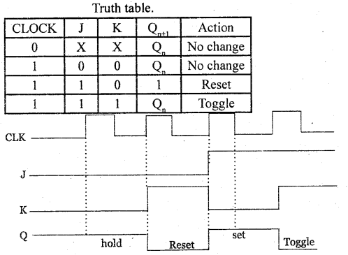
Explain the working of JK flip – flop with logic circuit. Draw its timing diagram and write its truth table.
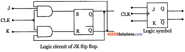
Answer:
- When J = 0, K= 0, the S and R inputs are both at 0 and hence the output is in the HOLD state.
- When J = 0, K = 1, S input is at 0 while R can be either at 0 or 1, but output is always in the RESET state.
- When J = 1, K = 0, S input can be 0 or 1 but R input is always at logic 0 and hence the output remains at a stable SET state.
- When J = 1, K = 1 the Flip flop goes to complementary’ state of previous output i.e, flip flop toggles
Question 36.
(a) Why 8051 microcontroller is known as 8 bit processor?
Answer:
8051 is called 8 bit processor because most of the operations are limited to 8 bits.
(b) Name the addressing modes of the following instruction.
MOV A, R0
MOV Ro, 40H
MOV A, @R0
Answer:
(i) Register addressing mode.
(ii) Direct addresssing mode.
(iii) Indirect addressing mode.
Question 37.
(a) Write a C program to accept the three integers and print the largest amongst them.=
Answer:
# include < stdio.h>
void main ( )
{
int x,y,z;
print f (” Enter the values of x, y, z\ n”);
scan f (” %d %d %d”, & x, &y, &z);
if (x > y)
if (x > z)
print/(‘x is largest /n”);
else
Print f (“z is largest/»”);
else if (y> z)
print f (“y is largest / rt” 0:
else
print f (” z is largest W);
}
/* End ofprogram * /
![]()
(b) Mention any four operators used in C programming.
Answer:
- Arithmetic operators.
- Relational operators.
- Assignment operators.
- Conditional operators.