You can Download Chapter 14 Semiconductor Electronics: Materials, Devices and Simple Circuits Questions and Answers, Notes, 2nd PUC Physics Question Bank with Answers, Karnataka State Board Solutions help you to revise complete Syllabus and score more marks in your examinations.
Karnataka 2nd PUC Physics Question Bank Chapter 14 Semiconductor Electronics: Materials, Devices and Simple Circuits
2nd PUC Physics Semiconductor Electronics: Materials, Devices and Simple Circuits NCERT Text Book Questions and Answers
Question 1.
In an n-type silicon, which of the following statement is true:
(a) Electrons are majority carriers and trivalent atoms are the dopants.
(b) Electrons are minority carriers and pentavalent atoms are the dopants.
(c) Holes are minority carriers and pentavalent atoms are the dopants.
(d) Holes are majority carriers and trivalent atoms are the dopants.
Answer:
An n-type semiconductor is obtained by doping a semiconductor with a pentavalent impurity. The impurity so added produces free electrons. Therefore, in an n-type semiconductor, the electrons are majority carriers and holes are minority carriers and pentavalent atoms are the dopants. Hence, the option (c) is correct.
Question 2.
Which of the statements given in Exercise 14.1 is true for p-type semiconductors.
Answer:
A p-type semiconductor is obtained by doping a semiconductor with a trivalent impurity. The impurity so added produces holes. Therefore, in a p-type semiconductor holes are majority carries and trivalent atoms are the dopants. Hence, the option (d) is correct.
Question 3.
Carbon, silicon and germanium have four valence electrons each. These are characterised by valence and conduction bands separated by energy band gap respectively equal to (Eg)c, (Eg)Si and (Eg)Ce. Which of the following statements is true?
(a) (Eg)Si < (Eg)Ge < (Eg)c
(b) (Eg)c < (Eg)Ge > (Eg)Si
(c) (Eg)c > (Eg)Si > (Eg)Ge
(d) (Eg)c = (Eg)Si = (Eg)Ge
Answer:
Carbon is insulator and hence the value of energy band gap is maximum for it. Of the other two semiconductors, the value of energy band gap for germanium is lesser. Hence, the option (c) is correct.
![]()
Question 4.
In an unbiased p-n junction, holes diffuse from the p-region to n-region because
(a) Free electrons in the n-region attract them.
(b) They move across the junction by the potential difference.
(c) Hole concentration in p-region is more as compared to n-region.
(d) All the above.
Answer:
In an unbiased p-n junction, hole concentration in p-region is more as compared to n-region. Hence, the option (c) is correct.
Question 5.
When a forward bias is applied to a p-n junction, it
(a) Raises the potential barrier.
(b) Reduces the majority carrier current to zero.
(c) Lowers the potential barrier.
(d) None of the above.
Answer:
When a p-n junction is forward biased, the applied voltage opposes the barrier voltage across the junction. As a result, the potential barrier gets lowered. Hence the option (c) is correct.
Question 6.
For transistor action, which of the following statements are correct:
(a) Base, emitter and collector regions should have similar size and doping concentrations.
(b) The base region must be very thin and lightly doped.
(c) The emitter junction is forward biased and collector junction is reverse biased.
(d) Both the emitter junction as well as the collector junction are forward biased.
Answer:
When emitter junction is forward biased, electron hole recombination takes place, the base region. To ensure that only a small amount (about 50%) of electron-hole recombination may take place the base is made thin and lightly doped. Hence the option (b) is correct.
Question 7.
For a transistor amplifier, the voltage gain
(a) Remains constant for all frequencies.
(b) Is high, at high and low frequencies and constant in the middle frequency range.
(c) Is low at high and low frequencies and constant at mid frequencies.
(d) None of the above.
Answer:
In a transistor, the voltage gain is high at high and low frequencies and constant at mid frequencies. Hence the option (c) is correct.
Question 8.
In half-wave rectification, what is the output frequency if the input frequency is 50 Hz. What is the output frequency of a full-wave rectifier for the same input frequency.
Answer:
- In half wave rectifier, the frequency of the output is same as that of the input i.e. 50 Hz.
- In full-wave rectifier, the frequency of the out put is twice as that input i.e 100Hz.
![]()
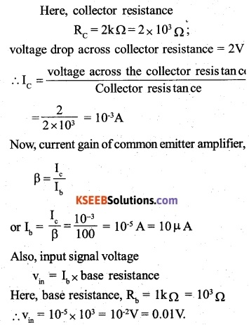
Question 9.
For a CE-transistor amplifier, the audio signal voltage across the collected resistance of 2kQ is 2 V. Suppose the current amplification factor of the transistor is 100, find the input signal voltage and base current, if the base resistance is 1 kQ.
Answer:
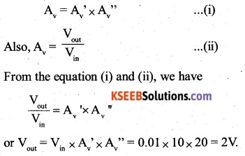
Question 10.
Two amplifiers are connected one after the other in series (cascaded). The first amplifier has a voltage gain of 10 and the second has a voltage gain of 20. If the input signal is 0.01 volt, calculate the output ac signal.
Answer:
When the amplifiers are connected in series, the net voltage gain (Av) is equal to the product of the gains of the individual amplifiers i.e.
Question 11.
A p-n photodiode is fabricated from a semiconductor with band gap of 2.8 eV. Can it detect a wavelength of 6000 nm?
Answer:
Here, λ = 600 nm = 600 x 10-9m
Therefore, energy associated with the wavelength,
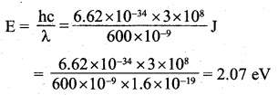
As the energy associated with the wave length is less than the band gap energy of the semiconductor, it can’t detect this wave length.
2nd PUC Physics Semiconductor Electronics: Materials, Devices and Simple Circuits Additional Exercises
Question 12.
The number of silicon atoms per m3 is 5 x 1028. This is doped simultaneously with
5 x 10²² atoms per m3 of Arsenic and 5 x 10²⁰ per m3 atoms of Indium. Calculate the number of electrons and holes. Given that n. = 1.5 x 10¹⁶ m-3. Is the material n-type or p-type?
Answer:
Arsenic is donor, where as indium is acceptor impurity. Here, number of donor atoms added,
ND = 5 ×10²²m3 and number of acceptor atoms added,
NA= 5× 10²⁰ m-3
Therefore, number of free electrons created, n=ND=5x10²² and number of holes created, nh = NA=5 x 10²⁰ .
Now, ne > nh
Therefore, net number of free electrons created
n‘e = n -nh = 5 x 10²² -5 x 1020
= 4.95 x 10²²m-3
Also, net number of holes created,
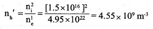
As \({ n }_{ e }^{ 1 }>{ n }_{ h }^{ 1 }\) the resulting material is n-type semiconductor.
![]()
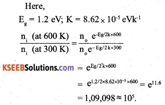
Question 13.
In an intrinsic semiconductor the energy gap Eg is 1.2eV. Its hole mobility is much smaller than electron smaller than electron mobility and independent of temperature. What is the ratio between conductivity at 600K and that at 300K? Assume that the temperature dependence of intrinsic carrier concentration n. is given by
\({ n }_{ 1 }={ n }_{ 0 }exp\left( -\frac { { E }_{ g } }{ 2{ k }_{ B }\quad T } \right) \)
where n0 is a constant.
Answer:
Question 14.
In a p-n junction diode, the current I can be expressed as
\(I={ I }_{ 0 }exp\left( -\frac { eV }{ 2{ k }_{ B }\quad T } -T \right) \)
where I0 is called the reverse saturation current, V is the voltage across the diode and is positive for forward bias and negative for reverse bias, and I is the current through the diode, kB is the Boltzmann constant (8.6×10⁻⁵ eV/K) and T is the absolute temperature. If for a given diode I0 = 5 x 10-12 A and T = 300 K, then
(a) What will be the forward current at a forward voltage of 0.6 V?
(b) What will be the increase in the current if the voltage across the diode is increased to 0.7 V?
(c) What is the dynamic resistance?
(d) What will be the current if reverse bias voltage changes from 1 V to 2 V?
Answer:
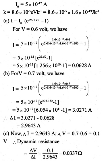
(d) For change in voltage from 1 to 2V, the current will remain equal to I0 = 5 x 10-12 It shows that the diode possesses practically infinite resistance in reverse biasing.
![]()
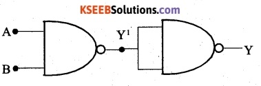
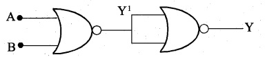
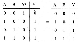
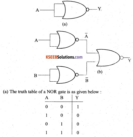
Question 15.
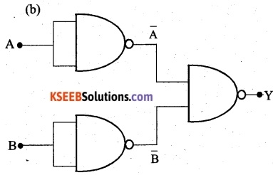
You are given the two circuits as shown in Fig. 14.44. Show that circuit (a) acts as OR gate while the circuit (b) act as AND gate
Answer:
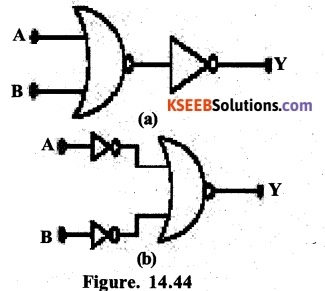
Answer:
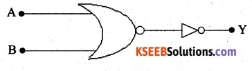
The output of NOR gate is connected to NOT gate. Let Y1 be the output of NOR gate and the final output of the combination of the two – gates be Y. The out put of NOR gate is 1 only when both the inputs are zero, while in NOT gate, the input gets inverted. Using these facts, the truth table for the given arrangement can be written as below :
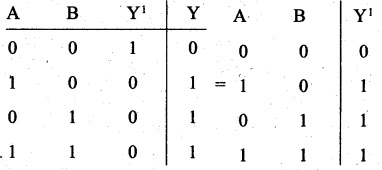
It is the truth table of OR gate. Therefore, the given circuit acts as Or gate
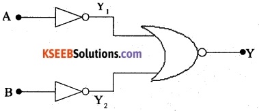
The output of two NOT gates are connected to NOR gate Let Y1 and Y2 be the outputs of the two NOT gates and the final output of the combination of three gates be Y. In a NOT gate, the input gets inverted, while the out put of a NOR gate is 1 only when both the inputs are zero. Using these facts, the truth table for the given arrangement can be written as below:
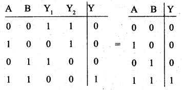
It is the truth table of AND gate. Therefore, ‘ the given circuit acts as AND gate.
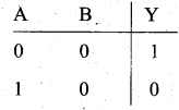
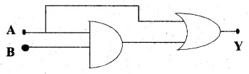
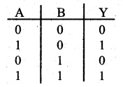
Question 16.
Write the truth table for a NAND gate connected as given in Fig. 14.45.
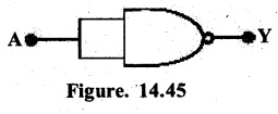
Hence identify the exact logic operation carried out by this circuit.
Answer:
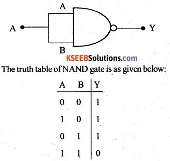
When the two inputs of a NAND gates are joined as shown in Figure i.e. when A = B = 0 or A= B = 1, the above truth table of the NAND gate reduces to the one as given below :
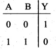
It is the truth table of a NOT gate. There operation of a NOT gate.
Question 17.
You are given two circuits as shown in Fig. 14.46, which consists of NAND gates. Identify the logic operation carried out by the two circuits.
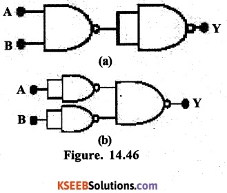
Answer:
Here, the output of NAND gate is connected to NOT gate [obtained from NAND gate]. Let Y1 be the output of NAND gate and final out put of the combination of two gates be Y. The out put of a NAND gate is 0 only when both the inputs are zero, while in NOT gate, the input gets inverted. Using these facts, the truth table for the given arrangement can be written as below.
It is the truth table of AND gate. Therefore the given Circuit acts as AND gate.
Here, the out puts of the NOT gates (obtained from NAND gates) are connected to NAND gate. Let Y: and Y2 be the outputs of the two NOT gates and the final out put of the combination of three gates be Y. In a NOT gate, the input gates inverted. While the out put of a NAND gate is 0 only when both the inputs are zero. Using these facts, the truth table for the given arrangement can be written as below:
It is the truth table of OR gate. Therefore, the given acts as OR gate.
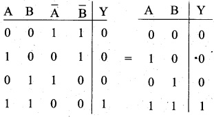
Question 18.
Write the truth table for circuit given in Fig. 14.47 below consisting of NOR gates and identify the logic operation (OR, AND, NOT) which this circuit is performing.
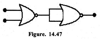
(Hint: A = 0, B = 1 then A and B inputs of second NOR gate will be 0 and hence Y=l. Similarly work out the values of Y for other combinations of A and B. Compare with the truth table of OR, AND, NOT gates and find the correct one.)
Answer:
Here, the out put of NOR gate is connected to another NOR gate, whose inputs are short- circuited. Let Y1 be the output of NOR gate and the final out put of a NOR gate is 1 only when both the inputs are zero. Using this facts, the truth table for the given arrangement can be written as below :
It is the truth table of OR gate therefore, the given circuit acts as OR gate.
![]()
Question 19.
Write the truth table for the circuits given in Fig. 14.48 consisting of NOR gates only. Identify the logic operations (OR, AND, NOT) performed by the two circuits.
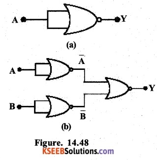
Answer:
When the two inputs of NOR gates are joined as shown in Fig (a) i.e.when A = B = 0or A = B = 1, the above truth table of the NOR gate reduces to the one as given below :
It is the truth table of a NOT gate. Therefore, the given circuit carries out the logic operation of a NOT gate.
Refer to Fig (b). Here the out put of two NOT gates (obtained from NOR gates) are connected to NOT gate. In a NOT gate, the input gets inverted. Let \(\bar { A } and\quad \bar { B } \) be the outputs of the two NOT gates. Now, the output of a NOR gate is 1 only when both the inputs are zero. Using this fact, the truth table for the given arrangement can be written as below :
It is the truth table of AND gate. Therefore, the given circuit acts as AND gate.
2nd PUC Physics Semiconductor Electronics: Materials, Devices and Simple Circuits Additional Questions and Answers
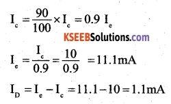
Question 1.
In a p-n-p transistor circuit, the collector current is 10mA. If 90% of the holes reach the collector, find emitter and base current. ‘
Answer:
Since 90% of the holes reach the collector
Question 2.
In input resistance of a transistor is 1000Ω. On changing its base current by 10μA, the collector current increases by 2mA. If a load resistance of 5 kΩ is used in the circuit, calculate
(i) current gain and
(ii) voltage gain of the amplifier.
Answer:
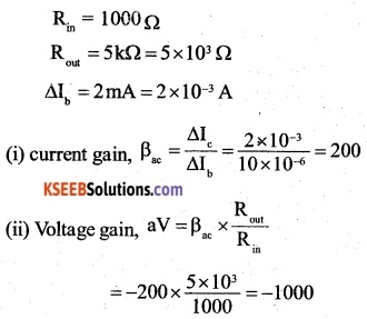
The negative sign shows that output is out of phase with the input.
Question 3.
State two disadvantage of semiconductor devices.
Answer:
- The semiconductor devices are temperature sensitive. Even a small overheating may cause damage to them.
- The semiconductor devices cannot handle as much power as ordinary vacuum tubes can do.
Question 4.
Express by a truth table, the output Y for all possible inputs A and B in the logic as shown
Answer:
Question 5.
The inputs A, B as shown are fed a 2-input NAND gate
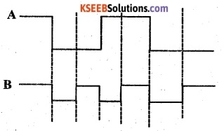
Draw the output waveform of the gate
Answer:
Question 6.
The valence electron in a alkali metal is a
(A) f-electron
(B) p-electron
(C) s-electron
(D) d-electron
Answer:
(C) s-electron
![]()
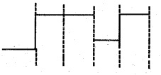
Question 7.
In which of the following figures, junction diode is forward biased?
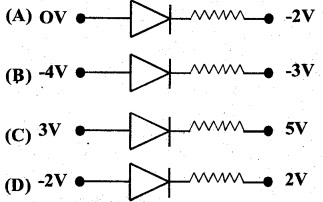
Answer:
(B).
During forward Bias, the p-section of the junction diode should be positive w.r.t the n-section.
Question 8.
The symbol shown in the adjoining figure is
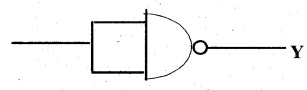
(A) NOT gate
(B) OR gate
(C) AND gate
(D) NOR gate
Answer:
(A) NOT gate
Question 9.
In a common base amplifier, the phase difference between the input signal voltage and the output voltage across collector and base is
(A) 0
(B) \(\frac { \pi }{ 4 } \)
(C) \(\frac { \pi }{ 2 } \)
(D) π
Answer:
(A) 0
Question 10.
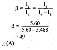
In a common base mode of a transistor, the collector current is 5.488 mA for an emitter current of 5.60 A. The value of the base current amplification factor (P) will be
(A) 49
(B) 50
(C) 51
(D) 48
Answer: