Students can Download 2nd PUC Electronics Model Question Paper 3 with Answers, Karnataka 2nd PUC Electronics Model Question Papers with Answers helps you to revise the complete Karnataka State Board Syllabus and score more marks in your examinations.
Karnataka 2nd PUC Electronics Model Question Paper 3 with Answers
Max Marks: 70
Time : 3 hrs. 15min.
Part – A
Answer all questions: 10 x 1 = 10
Question 1.
How many pn junctions are present in JFET?
Answer:
Two
Question 2.
Define DC load line.
Answer:
DC load line is a staight line on the output characteristics representing output dc voltage and corresponding direct current under no signal condition.
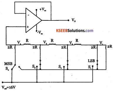
Question 3.
Draw the circuir diagram of a four bit R – 2R ladder network DAC.
Answer:
Question 4.
Define modulation index of an AM wave.
Answer:
Modulation index of AM is the ratio of amplitide of modulating signal to that of carrier wave.
![]()
Question 5.
How many sidebands are present in FM wave?
Answer:
Infinity
Question 6.
Mention one application of TRIAC.
Answer:
Light Dimmer.
Question 7.
Write the Boolean expression of XNOR gate.
Answer:
\(\mathrm{Y}=\mathrm{AB}+\overline{\mathrm{A}} \overline{\mathrm{B}}\)
Question 8.
Write the excess – 3 code of (304)10
Answer:
Oil 000110111 in Excess 3 code.
Question 9.
Which sign is used in as mnemonics for indirect addressing mode?
Answer:
@
Question 10.
Name the standard input and output functions used in C.
Answer:
Printf and scanf.
Part – B
Answer any five questions. 5 x 2 = 10
Question 11.
Write the advantages of voltage divider bias circuit.
Answer:
Voltage divider bias is the method of biasing a transistor. The voltage drop across forword biases the base emitter junction. This causes the base current and hence collector current to flow in zero signal condition and establishes operating point.
Advantages:
- It offers excellent stabilisation and hence Q point does not shift.
- when used in amplifiers, it provides better amplification.
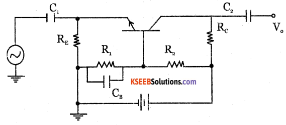
Question 12.
Mention the steps involved in drawing dc equivalent circuit of an amplifier.
Answer:
- Reduce all the AC sources to zero.
- open all the capacitors.
![]()
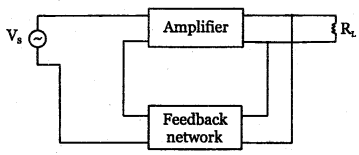
Question 13.
Draw the block diagrams of voltage series negative feedback and current shunt negative
feedback.
Answer:
(i) Current shunt negative feedback.
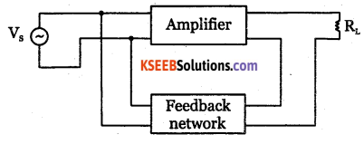
(ii) Voltage series negative feedback.
Question 14
Expand CMRR? Give its value for ideal op-amp.
Answer:
CMRR = Common mode Rejection Ratio
CMRR is infinity for Ideal Opamp.
Question 15.
Explain briefly the conditions of barkhausen criterion.
Answer:
- The total phase shift around the closed loop should be 0° or 360°.
- The magnitude of product of the open loop gain of the amplifier (A) and feedback ratio (P) is unity. Ie, | Aβ |= 1 .
Question 16.
What is the difference between MOVC and MOVX instructions of 8051?
Answer:
MOVX transfers data between’Accumulator and external data memory.
MOVC moves the byte from the code or program memory to the Accumulator
![]()
Question 17.
List the features of C language.
Answer:
C is a powerful, flexible language that has gained worldwide acceptance in recent years. C is concise, yet powerful in its scope. It is a high-level language that also incorporates features of low-level languages. It is becoming the standard for program development on small machines and microcomputers.
It is possible to apply C to nearly all application areas. Modularity {process of dividing problems into sub-problems) makes C ideal for projects involving several programmers. C permits nearly every programming technique. C is widely available for most brands and type of computers. It is portable. With all the features C is not a difficult language, it is one of the easiest languages to learn and implement.
C programming can be used to write any complex program because of its rich set of built-in functions and operations. C compiler combines the capabilities of an assembly language with the feature of high-level language and therefore it is very much suited for uniting both system software and business packages. Because of its variety of data types, powerful operator programs in C are efficient and fast. C has the ability to extend, it means user-defined functions can also be added to C library.
Question 18.
Distinguish between uplink and downlink signals.
Answer:
The transmission of a signal from an earth station to a satellite is called uplink. The retransmission of a signal from a satellite to an earth station is called the downlink.
Part – C
Answer any five questions. 5 x 3 = 15
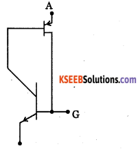
Question 19.
What are the functions of Drain, Source and Gate of JFET?
Answer:
Drain collects the charge carriers supplied by the source. Gate controls the flow of charge carriers through the channel.
![]()
Question 20.
With a block diagram, derive an expression for input impedance of an amplifier with negative feedback.
Answer:
An amplifier should have high input impedance so that it will not load the preceding stage or input voltage source. High input impedance for an amplifier can be achieved with Voltage series negative feedback.
Let Ii and Vi be input current and input voltage to the basic amplifier. Vs is input to feedback amplifier, Vf is feedback voltage and vo is the output voltage.
Input impedance of basic amplifier is
\(z_{i}=\frac{V_{i}}{I_{i}}-(1)\)
Input impedance of feedback amplifier is
\(z_{v}=\frac{V_{s}}{I_{i}} \rightarrow(2)\)
Input voltage to basic amplifier with negative feedback is
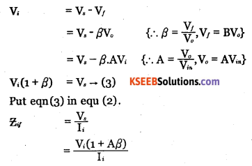
\(=\left(\frac{V_{i}}{I_{i}}\right)(1+A \beta)\)
Zif = Zi (1+Aβ)from eq ………… (1)
As (1 + Aβ) > 1 for negative feedback, Zif > Zi
Hence with negative feedback, input impedance of an amplifier increases.
Question 21.
Mention the characteristics of an ideal op-amp.
Answer:
| Characteristics | Ideal op amp | Practical op – amp |
| open loop gain | ∞ | 105 |
| Input impedance | ∞ | Few M Ω. |
| Output impedance | 0 | Few ohm. |
| Bandwidth | ∞ | Few MHz. |
| CMRR | ∞ | 90 dB |
![]()
Question 22.
Explain the importance of ionosphere in the radio communication.
Answer:
Ultraviolet radiation from the sun causes the upper atmosphere to ionize i.e. to become electrically charged. Hence a thick layer of ions formed at heights of 50 km to 400km. The ionosphere supports MF and HF wave propagation.
Its three layers are:
D layer: It is at a height of 70 km and has an average thickness of 10 km. It disappears in the night time. It reflects VLF and LF waves and absorbs MF and HF waves.
E layer: It is at a height of 100 km with a thickness of 25 km. This layer disappears at night. It helps in MF and HF wave propagation.
F layer: It is at a height of 150 km and extends up to 400 km. This layer exists during both day and night time. During day time, it splits into two layers F, and F2, and combines to form a single F layer during night time.
| F2 region. 250-400 km. |
| F1 region. 160-250 km. |
| E region. 95-130 km |
| D region. 50-95 km. |
| Troposphere Earth. |
Question 23.
Briefly explain the function of an AM diode detector.
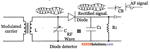
Answer:
LC tank circuit is used as a parallel resonant circuit. The resonant frequency of the circuit can be varied by varying the value of capacitance C and hence RF signal of any desired frequency can be tuned in.
When a selected modulated signal is applied to the diode, the diode conducts only during the positive half of the modulated wave. Thus the diode removes the entire negative half cycles. Across R1C1 only positive half cycles of carrier modulated wave appears. Thus the low pass filter made up of R1 C1 removes the RF.
During positive half cycle, diode conducts the capacitor C1 gets charged. During negative half cycle of the carrier and diode doesnot conduct but C1 discharges through R1. Hence output is obtained. The spikes can be reduced by proper choice of R1 C1 and depth of modulation. The capacitor CB removes Dc component produced by the detector.
![]()
Question 24.
A silicon power diode has V. (the drop across the p+n– junction) of 0.4V, RON (ohmic drop) in drift region of 0.002 Ω. Determine VAK if
(a) 1F = 75A and
(b) 1F = 100A.
Answer:
Vj= 0.4V, Ron = 0.002Q
VAK= Vj + VRD = Vj + RON If = 0.4 + 0.002 x 75 = 0.55V
VAK = Vj + VRD – Vj + RON If = 0.4 + 0.002 x 100 = 0.6V.
Question 25.
What is half – adder? Draw the logic diagram and truth table of half adder.
Answer:
| Inputs | Outputs | ||
| A | B | Sum Y = A⊕B | Carry Y = AB |
| 0 | 0 | 0 | 0 |
| 0 | 1 | 1 | 0 |
| 1 | 0 | 1 | 0 |
| 1 | 1 | 0 | 1 |

Question 26.
Mention any three uses of internet.
Answer:
- Using internet, access to required information is easy, economical, reliable and fast.
- With E-mail, messages reach destination with in minutes.
- E-mail can be sent and received from any place.
- Using E-mail, message can be sent to several persons simultaneously.
Part – D
Answer any Three questions :
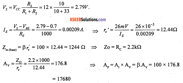
Question 27.
For a CE amplifier circuit, R1 = 33kQ, R2 = 10kQ, Rc = 2.2kQ, RE = 1kQ, RL = 10kfi,
Vcc= 10kv, β=100,VBE = 0.7V. Find IE ,=Zin(base),Zo and Av and AP Consider
\(r_{ e }=\frac { 26mV }{ l_{ E } }\)
Answer:
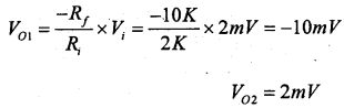
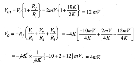
Question 28.
Calculate the output voltage in the circuit given below.
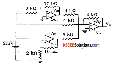
Answer:
Question 29.
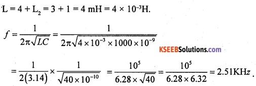
Calculate the frequency and feedback ratio of the circuit shown below.
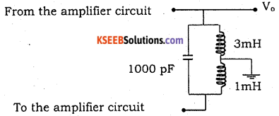
Answer:
Question 30.
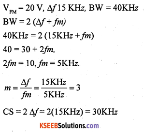
An FM signal of amplitude 20V with single tone modulation has a frequency deviation of 15 kHz and a band width of 40 kHz. Find the frequency of the modulating signal, modulation index and carrier swing. Write the expression of FM wave.
Answer:
Question 31.
Simplify the expression using K-map and draw the logic diagram for the simplified expression using NAND agates, given Y (A, B, C, D) = Σm (1,4,5,7,12,14,15) + Σd(3,6,13)
Answer:
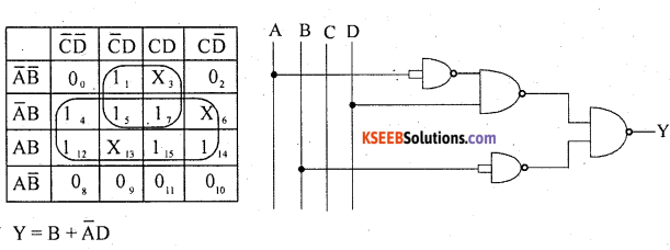
![]()
Part – E
Answer any Four questions. 4 x 5 = 20
Question 32.
With a circuit diagram explain the working of CB amplifier. Draw the input and output wave forms. Mention one application.
Answer:
The weak signal to be amplified is applied to emitter-base junction and output signal is taken across collector-base junction.
The DC power supply, R1, R2, RE, Rc provide the required biasing for the transistor. Capacitor C1, C2 block dc and allow ac to pass through. Capacitor CB by passes ac to the ground. During positive half cycle of input signal, the forward bias between base-emitter junction decreases, as VBE is already negative with respect to the ground.
Hence iE and ic. decrease and ic Rc also decreases.
VCB =Vcc – ic Rc . As ic Rc decreases, VCBincreases. Hence we get amplified positive half cycle. During negative half cycle of the input signal, forward bias is increased because VBEis negative w.r.t. the ground.
Hence iC , iE are increased and ic Rc is increased. As VCB =Vcc – ic Rc when ic Rc increases, output voltage VCB decreases.
Thus, the positive going input signal produces positive going output signal and negative going input signal produces negative going output signal. Hence in CB amplifier, the input and output signals are in phase.
Question 33.
Explain FM transmitter with a block diagram.
Answer:
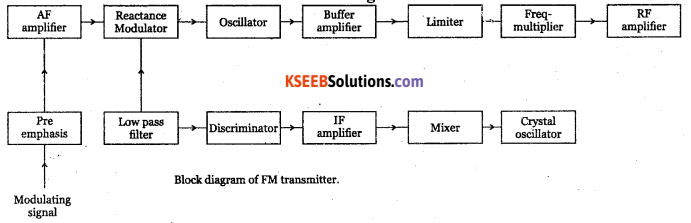
The modulating signal is applied to the pre-emphasis circuit, which improves signal to noise ratio, AF amplifier amplifies output of pre-emphasis. The processed signal is fed to reactance modulator. The reactance modulator uses a transistor or FET connected across tank circuit of carrier oscillator.
The oscillator frequency depends on the tank reactance which in turn depends on the instantaneous amplitude of modulating signal. Thus, output of reactance modulator will be a frequency modulated wave.
The oscillator is followed by a buffer amplifier which isolates oscillator from subsequent stages. The limiter maintains the amplitude constant. Class C power amplifier amplifies modulated wave to required power levels. The FM signal is then fed to the transmitting antenna.
![]()
Question 34.
With a sketch explain the two reansistor model of SCR. Derive an equation for anode
curent for zero gate current.
Answer:
When gate terminal is open, IG = 0. Then J1, and J3 are forward biased and J2 is reverse biased
Then Ic1 =α1 IA + ICu1 — (1)
Ic2 =α2 IA + ICu2 — (2)
α1,α2 are current gains of transistor Q1 and Q2
while ICu1 and ICu2 are reverse saturation currents.
We have IA = Ic1+ Ic2 — (3)
Equation (3) becomes,
IA = α1 IA + ICu1 + α2 Ik + Iω2 —-(4)
It = Ia + Ic = IA
Put Ik = IA .in equation (4),
IA = α1 IA + ICu1 + α2(IA +Ic ) +ICu2
Solving this equation,
\(I_{ A }=\frac { I_{ Cu1 }+I_{ Cu2 } }{ 1-\left( \alpha _{ 1 }+\alpha _{ 2 } \right) } +\frac { I_{ CO } }{ 1-\left( \infty _{ 1 }+\infty _{ 2 } \right) } \)
Where ICuo = ICu1+ ICu2
Question 35.
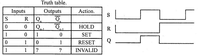
Explain the working of clocked RS flip-flop using NAND gates. Write its truth table and timing diagram.
Answer:
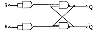
It is constructed using inverters inserted into inputs of cross coupled NAND gates.
Working:
- When S=0, R=0, it does not respond and hence outputs Q and Q will remain in their previous state. This is called HOLD condition.
- When S=1 and R=0, the output Q and Q change to 1 and 0. This condition is called SET state.
- When S=0, R=1, the output Q and Q change to 0 and 1. This condition is called RESET state.
- When S=1 and R=l, it drives output Q and Q both to HIGH which is FORBIDDEN or INVALID condition.
Question 36.
Write a program to add the values of locations 40H and 41H store the result in locations
50H and 51H.
Answer:
MOV A, 40H
ADD A, 41H
MOV 5 OH, A
MOV 51H, A.
Question 37.
Write the basic structure of C program and explain each section in brief.
Answer:
C program may contain one or more sections as shown in fig. 1.
Overview of a C program
| Documentation Section |
| Link Section |
| Definition Section |
| Global declaration Section |
| main( ) Function Section { Declaration part Executable part } |
| Subprogram Section Function 1 Function 2 Function 3 Function 4 ………………… (User-defined functions) Function n |